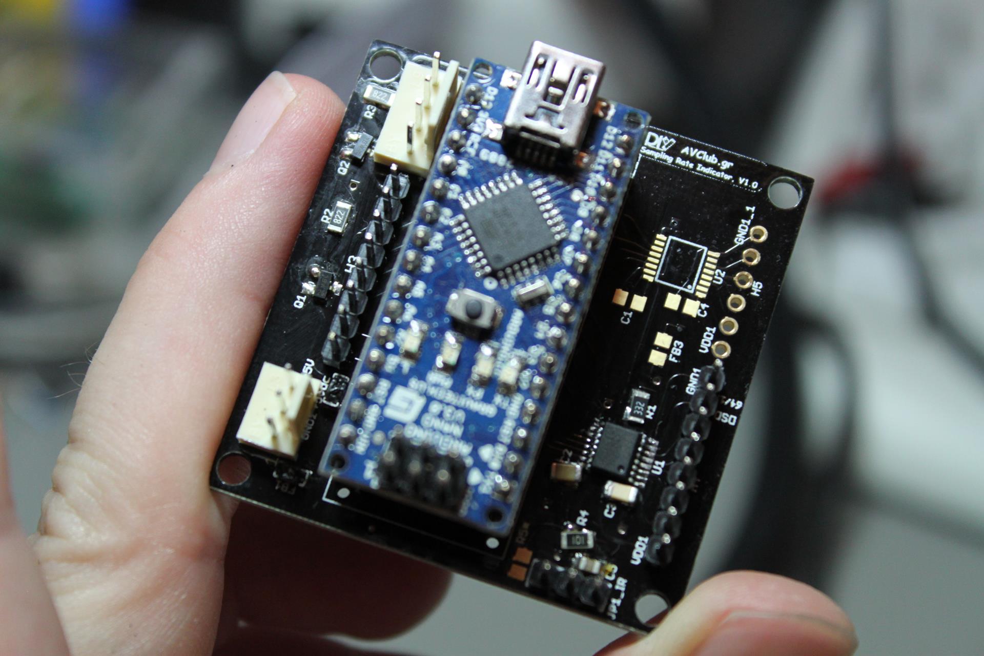
Over at avclub.gr we designed a custom PCB to ease the implementation of the Universal USB to I2S Interface Indicator. It was a joint effort between myself and Manolis (a.k.a. lemon at avclub.gr). I did the circuit design and Manolis did the PCB design work.
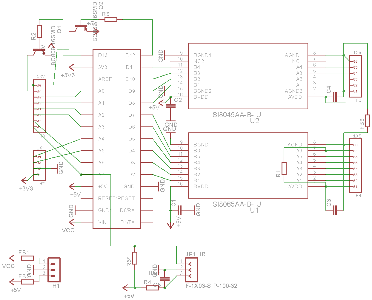
This is the schematic of the final version of the circuit:
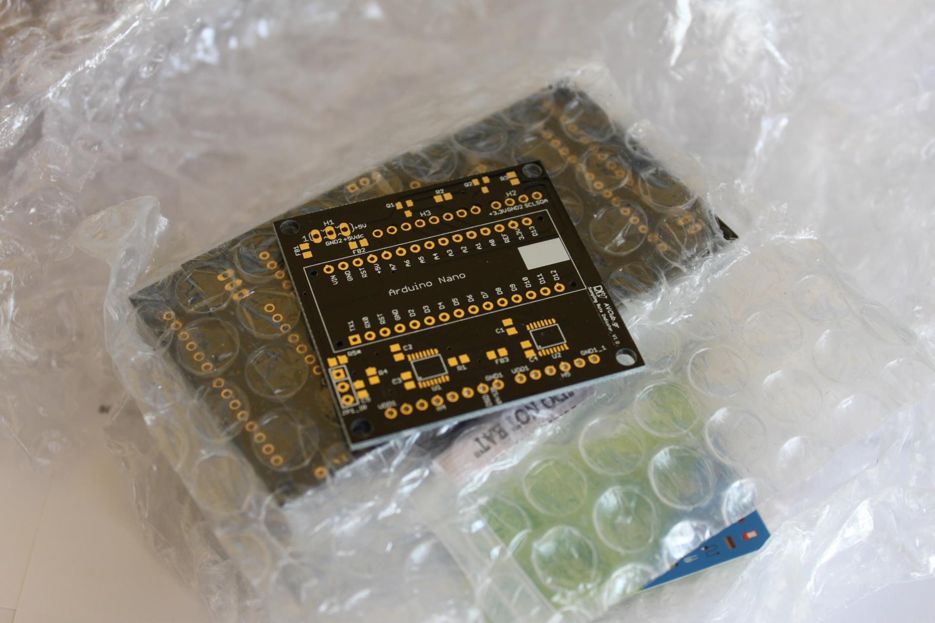
When the PCB design was finalized, a GB was organized. When the GB was finished we placed an order on seeedstudio.com’s Fusion PCB service. About 3 weeks later the PCBs had arrived:
 The production quality was truly excellent.
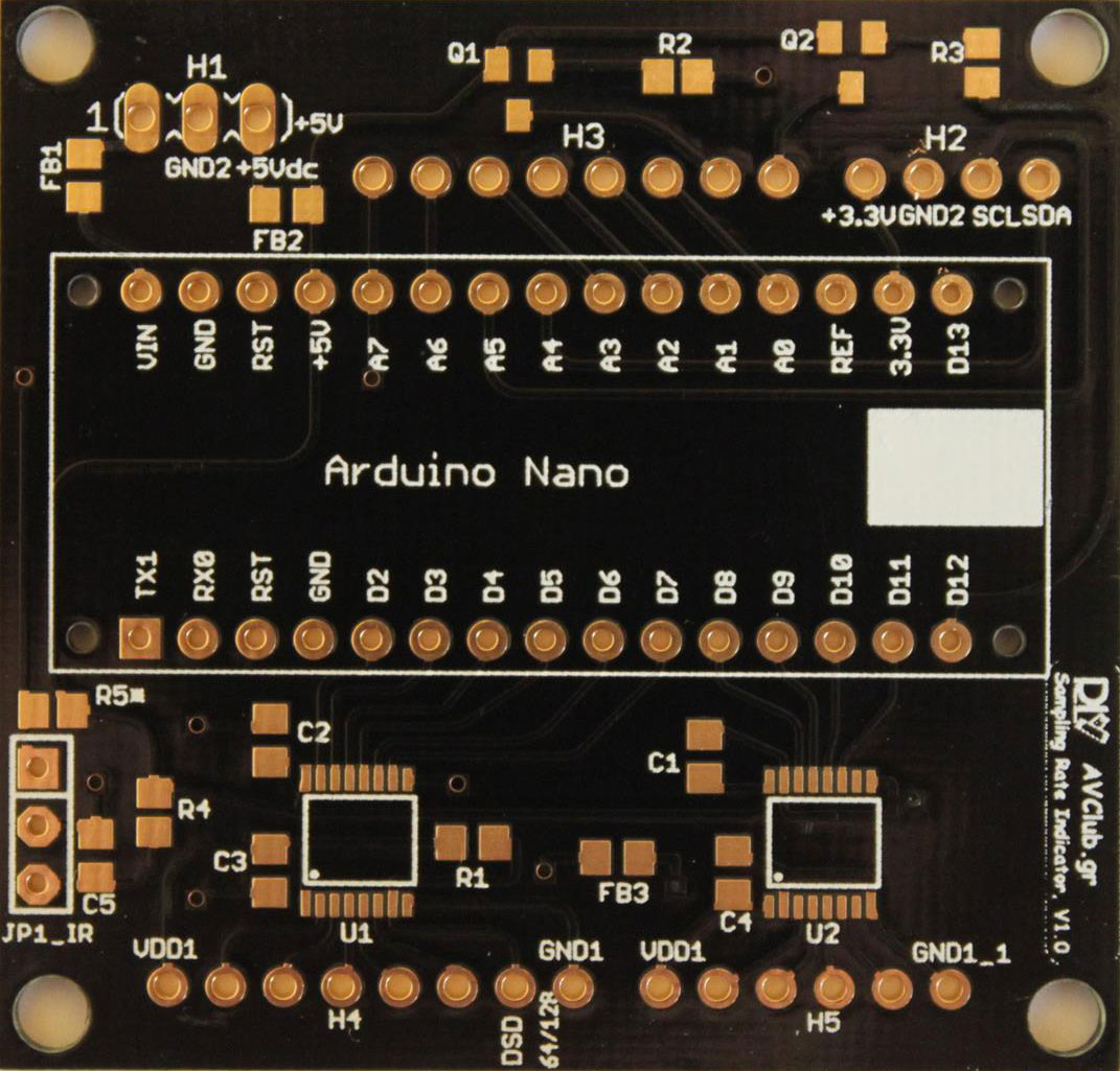
From top to bottom we have:
- H1: Header for power. It may be either 5VDC (regulated) or 7-12VDC (non-regulated). Pin 1 is 7-12VDC, Pin 2 is GND, Pin 3 is 5VDC.
- H2: OLED display connector. Pin 1 is 3.3V to the display, Pin 2 is GND, Pin 3 is SCL, Pin 4 is SDA.
- H3: Header for future expansion. It exposes the unused I/O of the Nano in case it may be of use in the future. The last two pins are buffered by transistors so that they can supply enough current to engage small relays (5VDC, up to 100mA per pin). Pin A7 is connected to JP1_IR as well (see below).
Next up is the socket for the Arduino Nano. You will notice that the USB port should be on the right.
At the bottom of the board we have:
- JP1_IR: This is a connector for an IR Receiver module. Software support for this is currently in beta. Pin 1 is signal out, Pin 2 is GND, Pin 3 is power (5V). Note that R4 and C5 provide filtering for the power and should be installed. R5 is an optional pull-up resistor. It should not be installed for normal use.
- H4: This is the “dirty” side of the U1 isolator. Pin 1 is Vdd (usually 3.3V or whatever your USB Interface module uses for its logic levels). Pins 2 through 7 are inputs and Pin 8 is GND.
- H5: This is the “dirty” side of the U2 isolator. Pin 1 is Vdd (usually 3.3V or whatever your USB Interface module uses for its logic levels). Pins 2 through 5 are inputs and Pin 8 is GND.
Note that in the future a Si8642BA may be used in place of U2. With proper support from the code that will turn 2 of the 4 inputs into outputs, so that they may be used to control a DAC board (for example to select an input).
This is the full BoM:
| Part | Description |
| FB1, FB2, FB3 | Ferrite Bead 0805 |
| R1 | 2.7K 0805 |
| R2, R3 | 8.75K 0805 |
| R4 | 100R 0805 |
| R5 | 10K 0805 (optional) |
| C1, C2, C3, C4 | 100n X7R 0805 |
| C5 | 10uF 10V X7R 0805 |
| Q1, Q2 | BC808 or equivalent SOT-23 |
| U1 | Si8065AA-B-IU |
| U2 | Si8045AA-B-IU (optionally Si8642BA-B-IU) |
In case you want to have your own PCBs made, these are the Gerber files: Universal USB to I2S Interface Indicator PCB Gerbers (21781 downloads )
You will also need an Arduino Nano, a suitable OLED display and some cables, connectors, etc. (see project page).
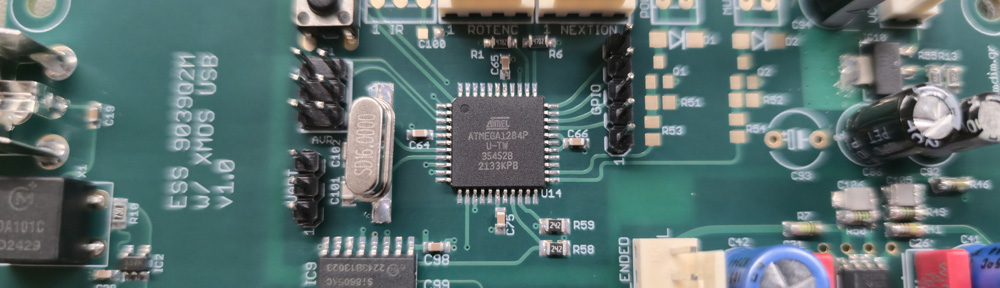
As soon as I received the boards, I built a prototype with whatever components I had lying around (thus the wrong size of most of the resistors & capacitors).
And proceeded to test it out with an Amanero Combo384 board:
Everything worked as it was expected. 🙂
At the moment this board (and relevant Arduino code) has been tested with the following USB to I2S interfaces:
Amanero Combo384
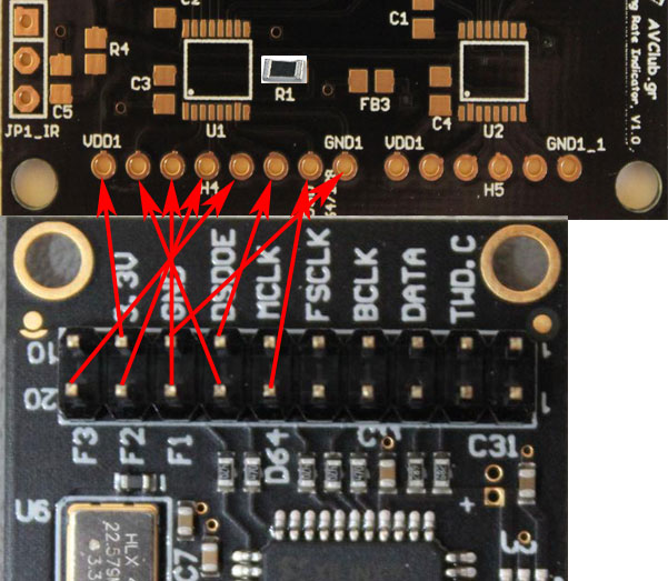 Note that R1 should be installed for proper operation.
DIYINHK XMOS
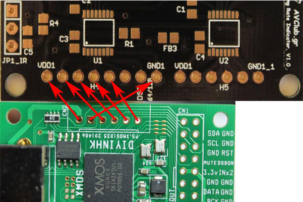
JLSounds I2SoverUSB
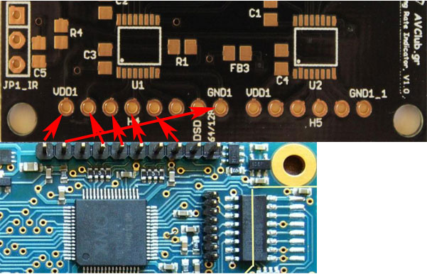
Luckit WaveIO
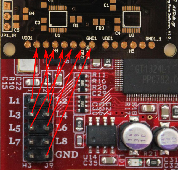
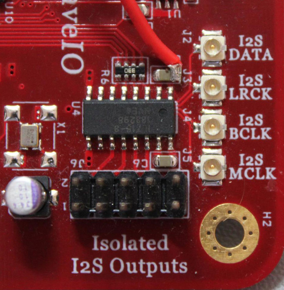
You will notice that there is no Vcc pin on J9. In order to power the isolator, we will have to “steal” power from elsewhere on the board. A good place to tap is the power pin of the on-board I2S isolator, just to the left of the I2S LRCK U.FL:
Would it be able to work with the uno as well?
I’m afraid not, at least not as a “shield”. But if you just need I2C or serial isolation you could just hardwire it.
Hello Dimitri,
do you happen to have any spare pcb of this project ?. I would love to build it.
best regards
Pepe
Hi there Pepe, I’m sorry but all of the boards are gone. I am considering though giving out the gerber files so you can order your own.
Hi there Dimitri,
thank you very much for adding the gerbers, I am ordering a pair of boards for myself right away.
Keep posting so great projects, I enjoy very much reading your research.
best regards
Pepe
Good evening DIMDIM,
I write from Italy. In this moment of COVID lockdown I am dedicating myself to the DAC project on JLSOUNDS boards.
Your Sample Rate Indicator for USB to I2S interfaces is very interesting for me!Unfortunately I do not have equipment to solder smd components…
Would it be possible to commission you a ready-made and tested card for I2SoverUSB Jlsounds DAC?
I would like to make a complete chassis DAC and the screen wiyh the frequency would be very nice!Click the image to open in full size.
Thanks a lot for your answer.
BR
Hi there,
COVID has given most of us some extra time to work on our projects, it’s the silver lining of this pandemic.
I’m afraid that this is just a hobby for me, I do not do this for a living. So all I can offer is a few spare unpopulated pcbs.
Best Regards from Greece!
Hi Dim and thaks for your answer.
I would be interested to pcb card.Is it possible to buy it?
Another question: Is programming the Arduino complicated? I don’t know him and I have to study him.
BR
Alberto
Hi Dimitri, Do you have news for the pcb? I’m very interested for this project.
Thanks
BR
Alberto
Frist thanks for sharing your gerber. I am considering this clock indicator my new DAC. But it seems the BOM link has gone. Would you provide the BOM again?
Regards.
From Korea
Hi there, fixed. 🙂