For the better part of a year I’ve been busy developing what one would call a “respectable” DAC from scratch. It has been a team effort, with different people becoming more involved with specific aspects of the project, but pretty much everyone involved ended up learning a lot about DACs. Right now, the project is for the most part finished, in that it is fully functional with a USB input and a pair of single ended outputs (or balanced, if you use a passive transformer-based stage). It is controlled by an Arduino-compatible micro-controller, running my aKduino v2 code (more on that in a future post).
I will do a series of posts detailing the design and build process, with each post covering a specific PCB. When the series is complete, the contents of all of the posts will be concatenated into a project page.
So, without further ado, this is the schematic of the main DAC board:
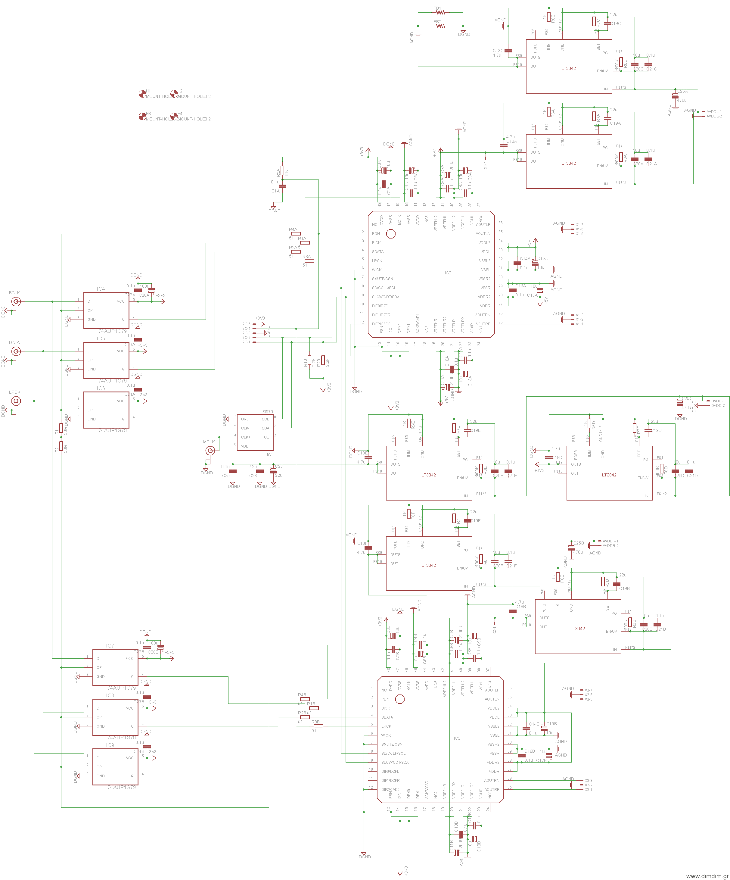 (Right click, Save Image As.. to download it in full resolution)
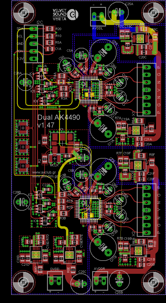
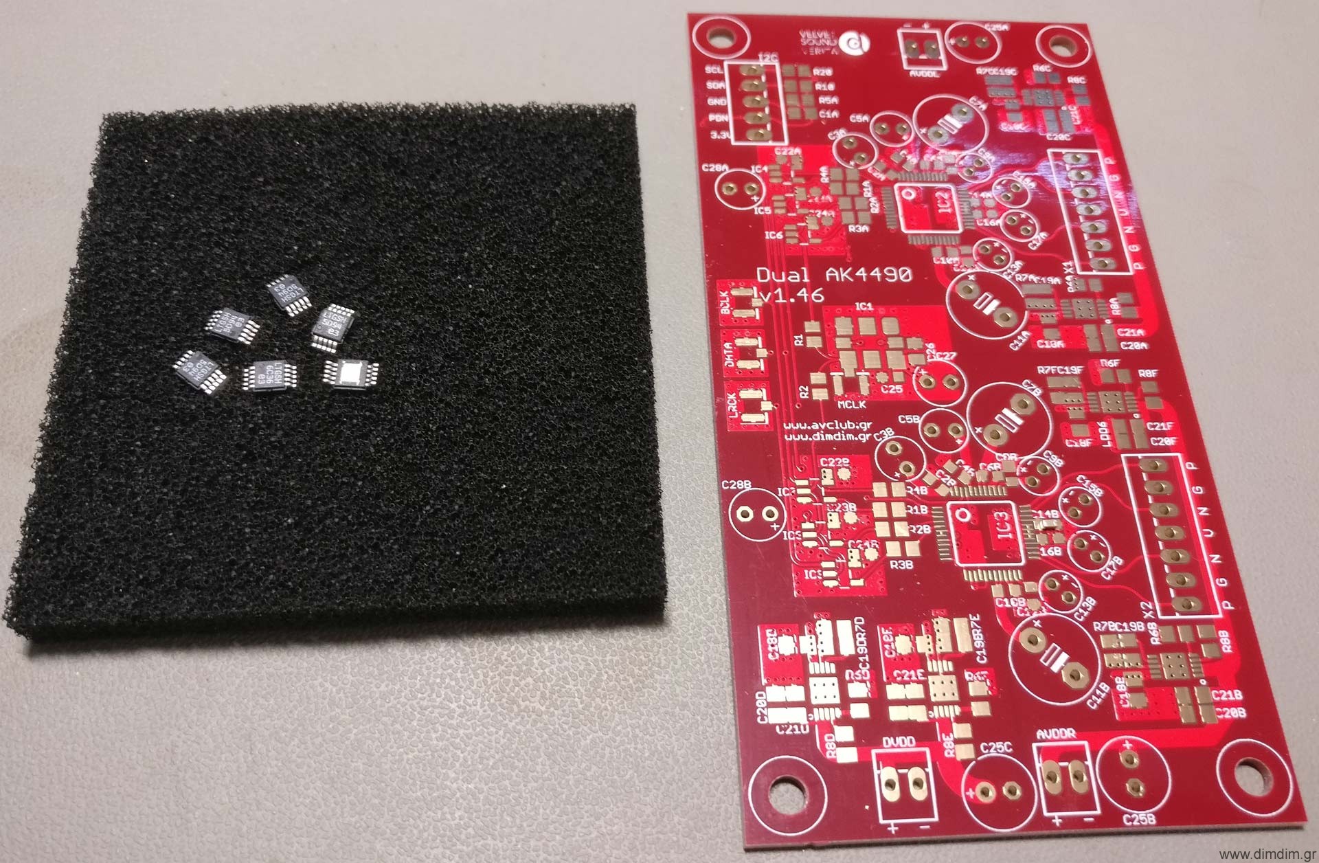
This is the 4-layer PCB:
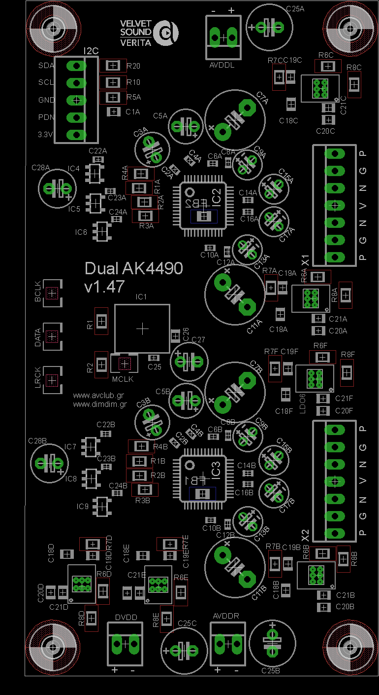
This is the parts placement diagram:
And this is the BoM (v1.9) in xls format: Dual AK4490 DAC (main board BoM) (19359 downloads )
Design considerations
The design goal was to do a dual mono design so as to maximize SNR and channel separation. A 4-layer PCB design was chosen so as to have a very solid, low impedance ground plane as well as proper power and signal planes. The I2S, audio signals and power after the local LDO regulators are routed on the top layer, the 2 middle layers are ground and power planes, and the bottom layer serves to route I2C signals and some power lines.
Power
All of the local power supplies are implemented using the currently top-of-the-line LT3042 LDOs. The VDDL & VDDR (analog power supplies) are set to 7.2V so as to maximize SNR and dynamic range. There is provision for providing separate pre-reg power supplies for the L and R channels (headers AVDDL and AVDDR) but I don’t consider that to be critical to SQ since there are local LDOs and the power draw is very very small. In my implementation I’m using a common pre-reg for both the AVDDL & AVDDR. The AVDDs and DVDDs are also supplied by LT3042 LDOs set to output 3.3V. The Si570 has its own dedicated 3.3V supply implemented with an LT3042 and features extra filtering.
Overall, the power requirements of the board are:
1) AVDDL: 8-10V DC at 40mA max
2) AVDDR: 8-10V DC at 40mA max
3) DVDD: 4-6V DC at 200mA max
Clocking & input signals
It was decided that the MCLK would be provided by a programmable low jitter oscillator, namely the Si570. This way we could select different MCLK frequencies at will, supporting different sampling rate families and different USB to I2S boards.
Speaking of USB to I2S boards, the DAC board has a very specific requirement: The USB board must be able to receive MCLK externally. In other words, the DAC board and USB board must be clocked from the same oscillator. This is due to the AK4490’s design. Unlike the ESS designs which by default run asynchronously, it needs to be on the same clock domain as its I2S sources.
So, the DAC board needs to output MCLK back to the USB board. There exist a number of USB boards that support that. The most popular ones are the Amanero Combo384 and JLsounds’ I2SoverUSB.
Since I had decided to do reclocking using flip-flops as close to the AK4490s as possible, and the flip-flops are clocked by the MCLK, its frequency needs to be sufficiently high in order to reclock signals corresponding to high sample rates. This translates to 49.152 MHz for sampling rates of 384KHz. If you’re content with going only up to 192KHz, you can use a MCLK of “just” 24.576 MHz. Of course you will also need the corresponding MCLKs of 45.1584 and 22.5792 MHz for the 44.1K families of SRs.
If you decide that you don’t want to do reclocking on the DAC board, you can just not solder on the flip-flops and just connect the proper pads together with some wire so as to bypass them. That way you can run with 22.5792 & 24.576 MHz clocks with SRs up to 384KHz (and probably beyond..).
If you decide that you would also prefer to not use the Si570 and just clock the DAC board directly from your USB to I2S board (or other suitable I2S source) you can also do that. You just don’t solder-on the Si570 and make a couple of changes to the Arduino code (to be implemented..).
But I urge you to try the Si570 & reclocking way first..
Construction hints
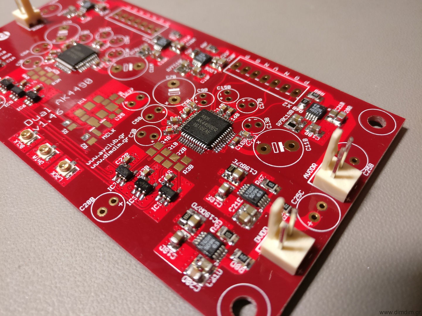
Start by first soldering on the power supply components (LDOs, resistors, caps, etc.) and testing that everything works the way that it should.
The LT3042s are pretty tiny and its easy to make a mistake while soldering them. I’ve found that the easiest method is by using a hot air rework station. First I use a regular soldering iron to tin the thermal pad and the pads with a small amount of solder. Then I apply a good amount of high quality solder paste, put the LDO on top of the pads and heat the area of the board until the solder melts. I set my hot air station to a relatively low temp of ~280 degrees C and the process takes less than a minute (per LDO). But you could also solder them with a soldering iron. To solder the heatpad, warm up the pad from the underside of the board and add solder.
After the power section, you should solder on the AK4490s and other low profile components. I do that with a low power (18W) soldering iron with a fine tip.
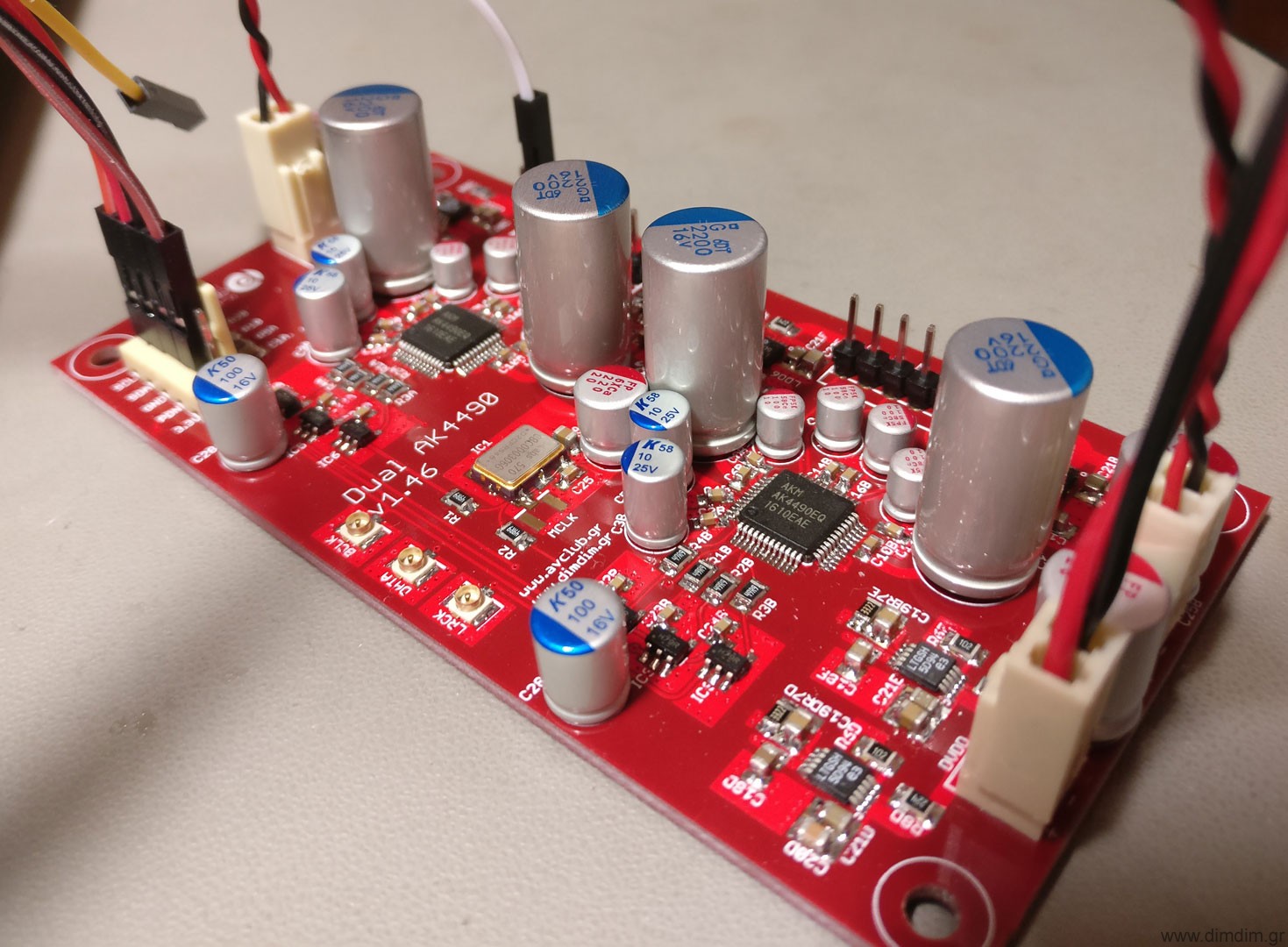
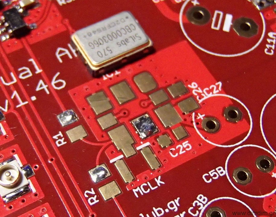
Next up is the Si570 programmable oscillator. I start by putting a little solder on one of the pads:
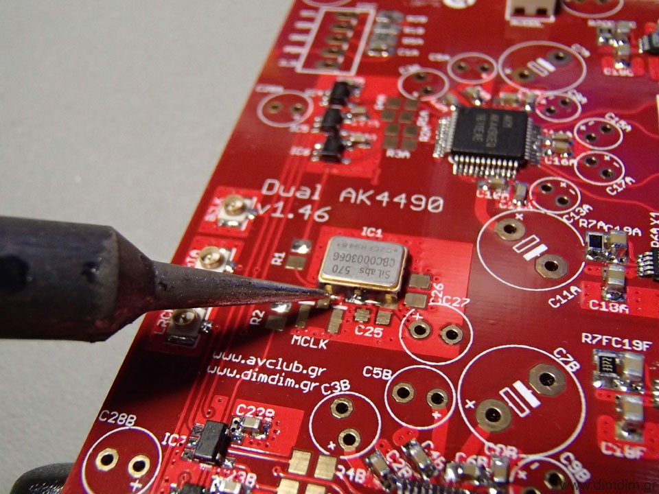
Then I add soldering paste and I place the Si570 on top of the pads. I use the fine tipped soldering iron to melt the solder on the tinned pad, effectively soldering the Si570 on the board. I then proceed to solder the rest of the pads by applying heat with the soldering iron to the side of the pads of the Si570 and adding solder.
You should finish up by soldering the electrolytic capacitors and other higher profile parts.
Beware that the spacing around the electrolytics is very tight. You should take that into account when selecting parts. The parts in the BoM are sure to fit in the available space.
That’s it for Part 1. Stay tuned for Part 2: The Controller.

Wow, that’s some neat stuff!
Ever though as releasing the i2s flip-flops reclock module with si570 as a standalone product (with buffering) ? 🙂
That wouldn’t really be practical because part of the effectiveness of the reclocking is because it (the flip-flops) and the Si570 are so close to the dac chips. That makes keeping trace inductances to a minimum, as well as controlling trace lengths, vias, etc.
If a standalone module was to be made, for it to work correctly it would need to clock the dac chip(s) and the I2S/spdif sources. That is not really practical in most cases.
Ian’s and Allo’s FIFO reclockers work because they use FPGAs with RAM to buffer the I2S signals, thus effectively separating completely the two clock domains (the I2S source and the DAC board have two completely different clock sources).
If you are going to make a second version you should look at getting trace width so that you get 50ohm line impedance. Damping / termination resistors closer to the source and maybe 0603 housing to get closer to the output pin of the LVC? Parts.
Br
Sonny / MIRAND
IIRC Eagle PCB does not afford such luxuries as calculating / simulating trace impedances.. I’ll have to look into that. Good point about the proper location of the termination resistors, as well as their size. I’ll definitely do that if there will be a second version or some other dac design.
Thanks Sonny. It’s really good to hear what the pros have to say about our (the hobbyists’) designs. 🙂
Excellent project & thanks for sharing.
Hey I notice you are not doing anything with the zero input detect pins (10, 11)
I find them very useful to control output muting to remove clicks/pops with track sample rate changes
Thank you for your kind words Clayton. 🙂
Are you getting clicks/pops during SR changes or just when switching between pcm & dsd? Because the only reason I’ve seen to add a muting relay is pcm & dsd switching, and I was planning to control that relay through software detection of signal type.
Yes the clicks/pops are mainly when going from DSD mode back to PCM.
I have hardware muting on the output stage using special muting transistors – transistors don’t quite give a full cutoff like a relay but are physically quite & softer switching with less less of a pop. The muting transistors are controlled by
1. Pin 11 from the Amanero
2. Zero input detect pins on the AK4490 (actually I’m using a AK4497 now)
Also I have been playing a little bit with soft mute in the DAC chip in my control code.
Software control is via a “stand alone” uno implementation using a Atmega 328P running on 3.3v to keep voltage level matching correct. My programming skills are not good so my son handles that.
Hey I know your programming skills are excellent so here is a project ideal for you – A USB to I2S board based on the Xmos XU208 – what do you think?
It would make a nice change from all the EBay ones.
Keep up the good work!
Cheers
Hi Dimdim? How soon will the second part?
Pretty soon.. I’m ironing out some bugs created by the latest updates to the stm32duino core.
Hi DimDim! Great project!
Are you planning to sell some PCB’s (or maybe share files – PCB design\gerber etc.) when it’ll be finished? And another interesting question – do you have a plans to try the new AK4493 with this project (when the AK4493 will be available, of course)?
Thanks in advance!
Hi there!
At the moment there exist 2 working DACs plus another 7 fellow DIYers are building this DAC. If they like the way it sounds, a GB might happen on diyaudio.com. Or I might just give out the gerbers, I don’t really know yet.
I looked into the AK4493, it looks like it’s an incremental upgrade from the 4490, but it’s not available yet commercially and knowing AKM’s track record it will probably be a few months before it becomes available. My board will need some relatively small modifications to become compatible with it. I can’t promise that I’ll go through with the upgrade, though.
BR,
Dimitris
Hey Dimitris, another great post:) I’m really looking forward to your controller code: I would love to adapt it for my Chinese dual ak4490 board instead of writing the whole thing from scratch 😉
Will you put it on github?
Hi there Sebastian!
The code is already up, on Part 2 of the story: http://www.dimdim.gr/2017/12/arduino-controlled-dual-mono-ak4490-dac-part-2/
I haven’t bothered getting familiar with Github yet..
Pingback: Arduino controlled Dual Mono AK4490 DAC (Part 2) | Dimdim's Blog
Pingback: Arduino controlled Dual Mono AK4490 DAC (part 3) - Electronics-Lab
Pingback: Dual Mono AK4493 DAC (MK II) | Dimdim's Blog
Hi.
do you think to make a project with AK4499EQ?
by the way what name do you have on diyaudio?
Pingback: A dual mono AK4493 DAC #Audio « Adafruit Industries – Makers, hackers, artists, designers and engineers!
Pingback: Dual Mono AK4493 DAC (MK II) – High Voltages News
Pingback: Digitalni sustav sa DSP skretnicom i 4-kanalnim DAC-om – igiBits
Hi !
I just discovered your site recently and I have spent about 2 weeks to see if I could able to fabricate a set by my own. It is possible sharing your PCB Gerber file to me ?
Hi there Benny,
I would have no problem sharing gerber files with you, but I would recommend my updated design with the AK4493s..
And of course you should double check that you can find the necessary components.. particularly the dac chips.
Hi DimDim,
Thank you and so glad to see your reply! : ) In fact, I have read your description of other projects ( e.g. TFT HiFiDuino Pro Project, Arduino controlled Dual Mono AK4490 DAC, Dual Mono AK4493 DAC (MK II …. ). Since I have no experience in DAC fabrication and your description of “Dual Mono AK4490 DAC” project which involves the DAC, Control panel, and Digital to Analog driver, it is relatively complete for me. So, after reviewing my capability, I think I should choose your “Dual Mono AK4490 DAC” project for my first step. I have also checked that it is not difficult to find the necessary components on my side.