 Time flies when you’re having fun. Or are just too busy with things, in general.
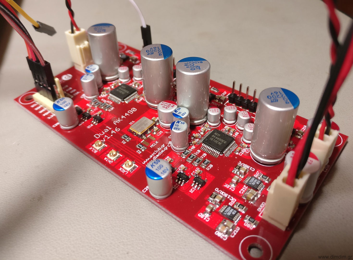
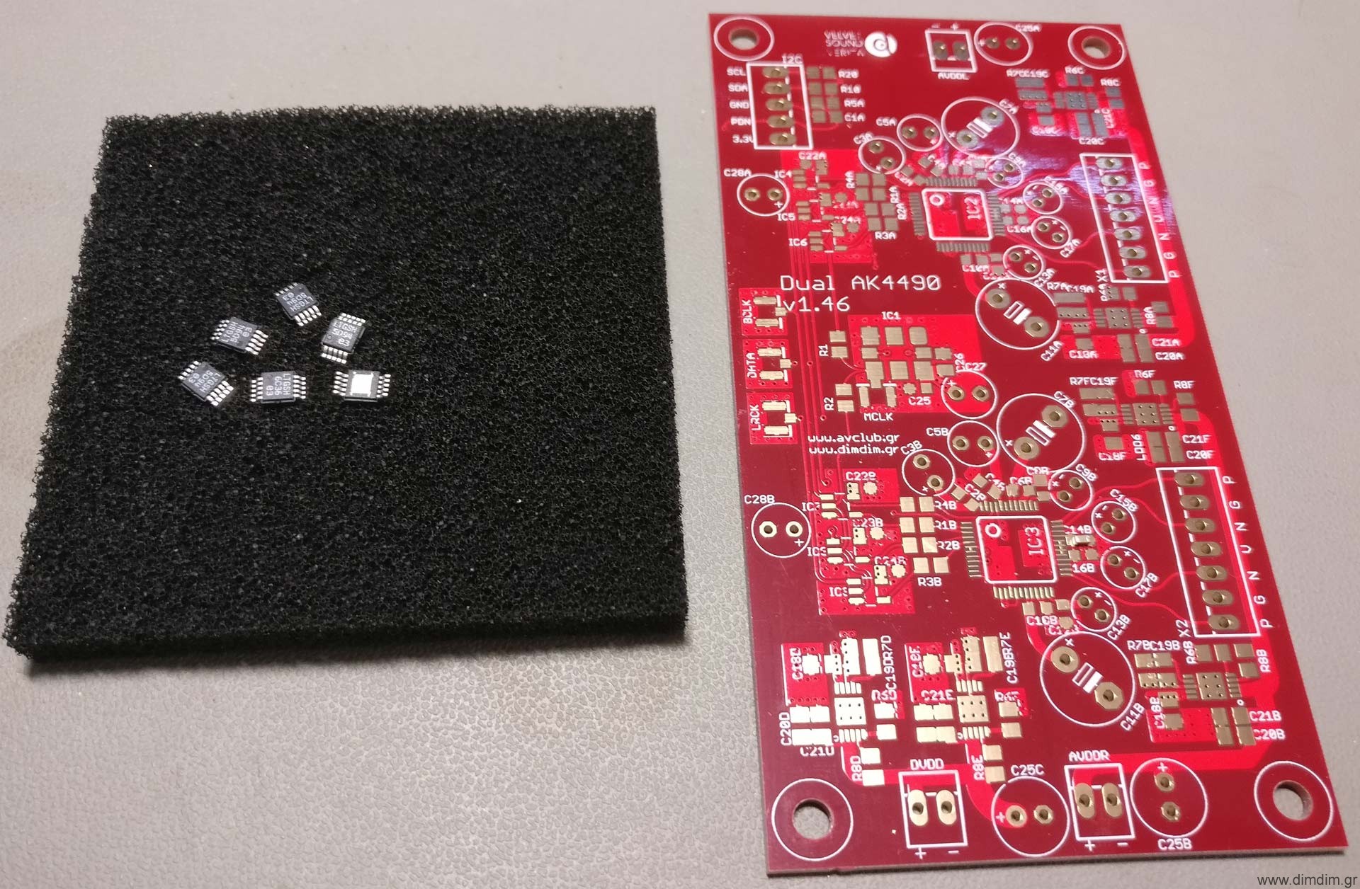
It’s been two and a half years since I posted about my Dual Mono AK4490 DAC. That DAC has been built and is in use by at least 6 people, other than myself. All of them have been very satisfied with its performance.
But since then quite some water has passed under the bridge.
Among other things, the AK4493 chip came out, and it was just that much different than the AK4490 that I had to update my design to accommodate it.
Feature-wise it was pretty enticing. It looked more like a limited performance version of the AK4497 than an upgraded version of the AK4490. So I had to try it out.
Since I was going to update the PCB design, I thought I might as well improve on as much as I could. So, the new board would:
- Include a new reclocking solution. I went for the best specc’ed chip out there, the famous Potato Semi PO74G374A. One chip would take care of the all of the I2S lines for both DAC chips.
- Add a couple of external 1.8V DVDD power supplies.
- Make some optimization of the LT3042 local regulators’ layout, in order to accommodate larger package capacitors (1206) where it would make most sense.
- Give access to the zero-detect lines of one of the dac chips. These pins could be used to easily implement auto muting of the output stage.
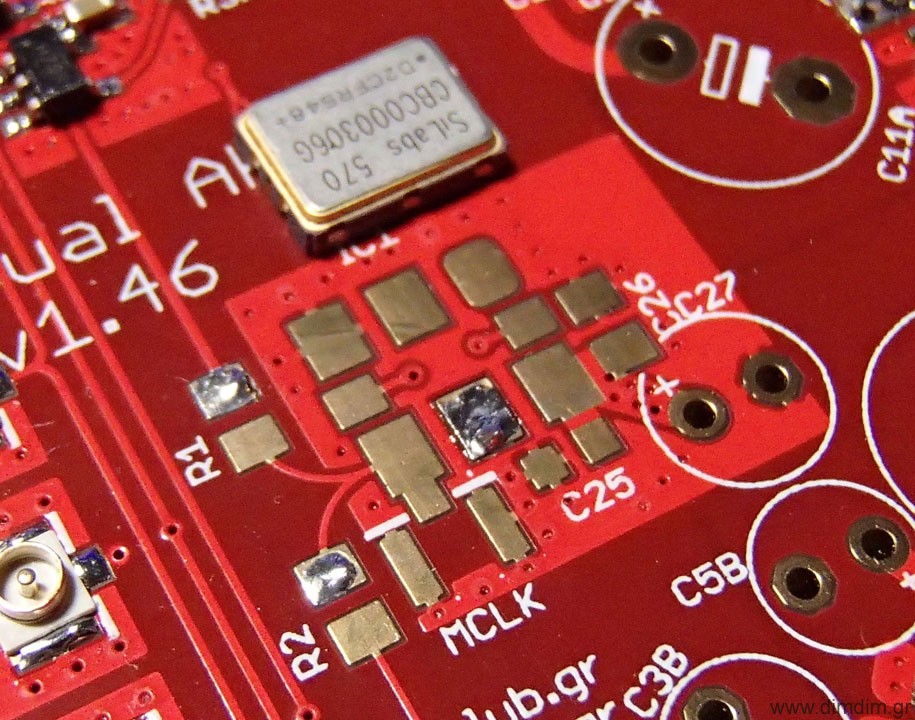
- Give access to the Enable pin of the Si570/Si544. The use of this Enable pin will be explained later.
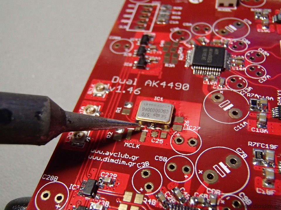
In addition I would use the then new Si544 programmable oscillator, offering improved performance over the Si570. This did not require any changes to the pcb.
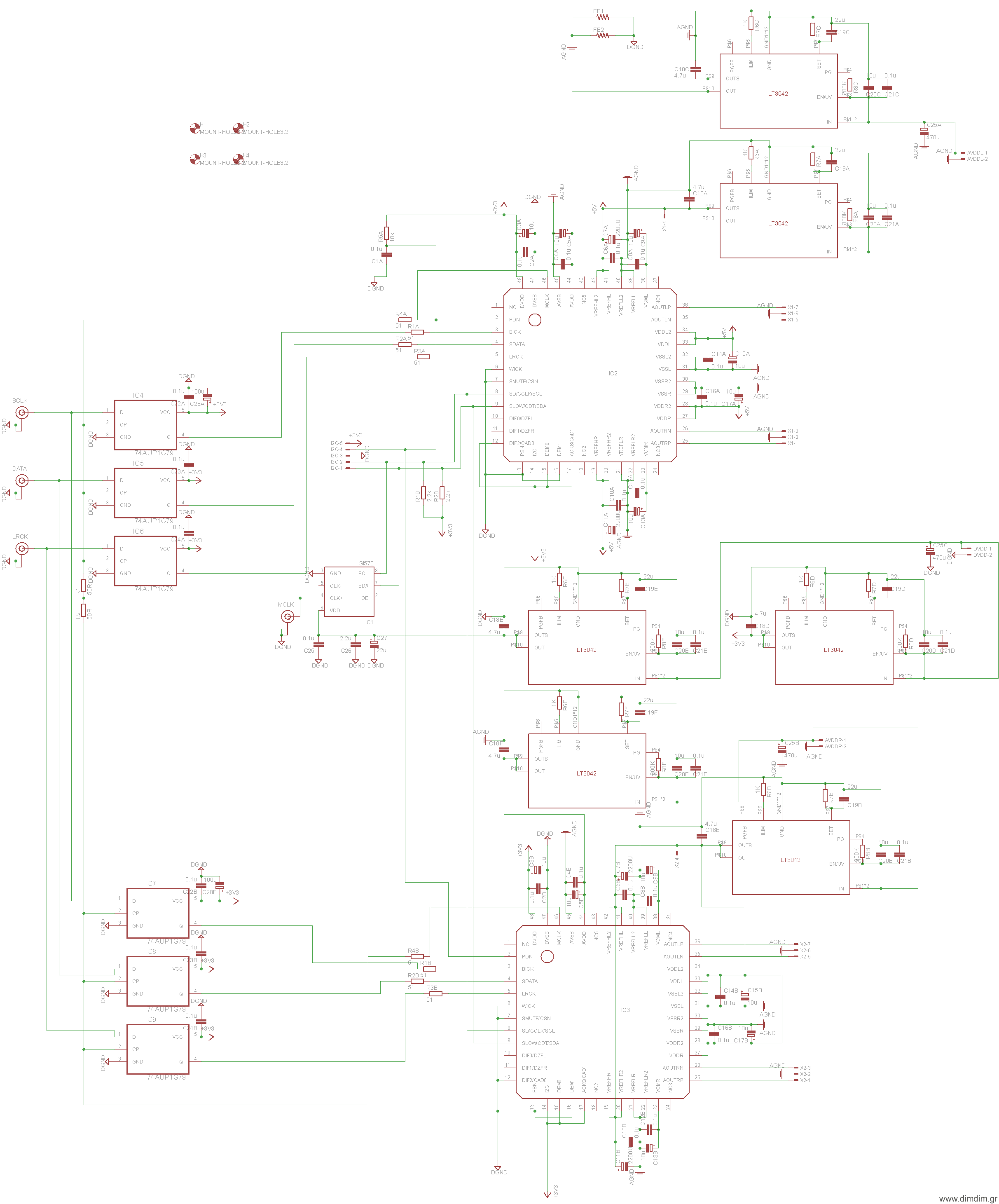
This is the updated schematic:
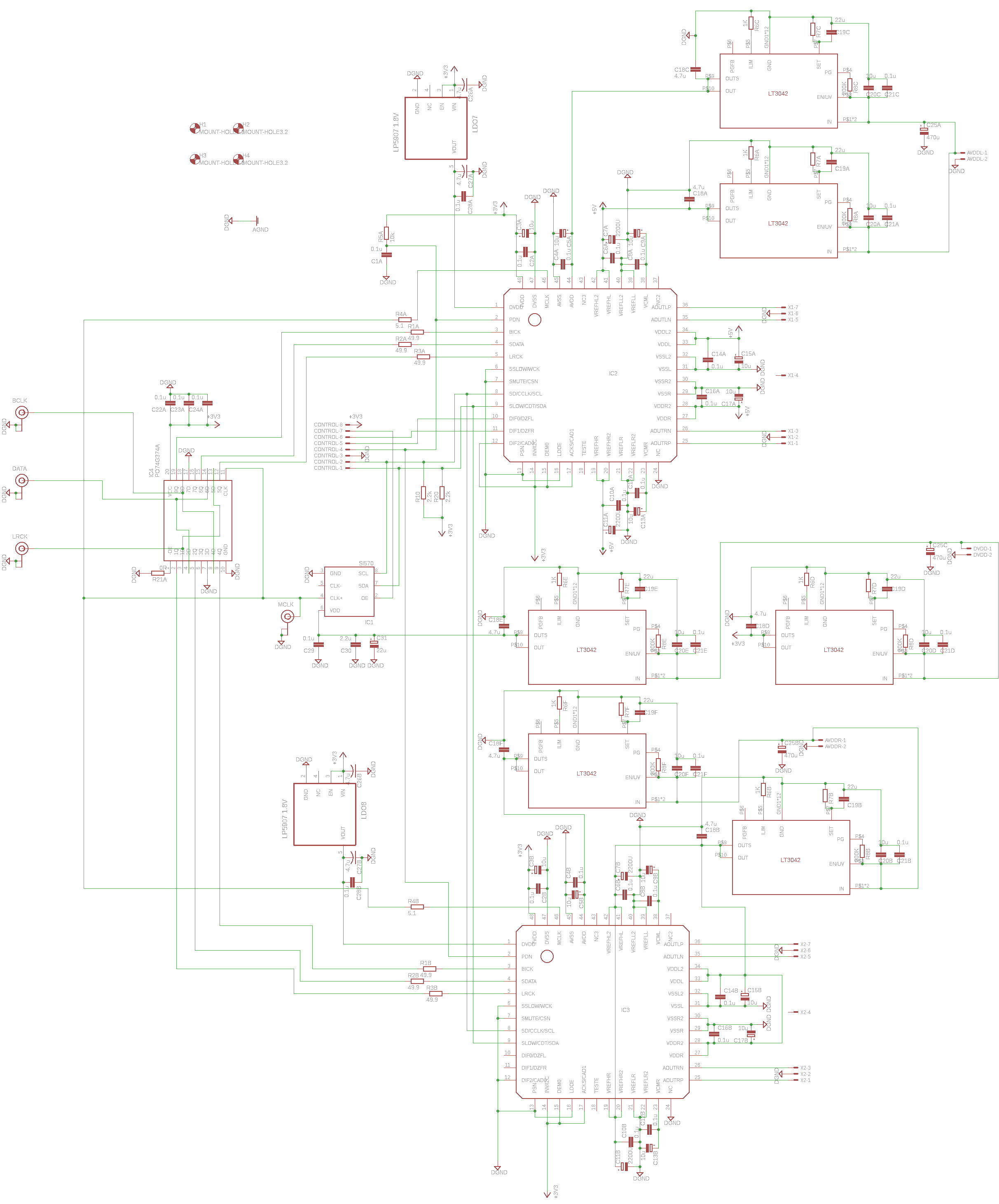 (Right click, Save Image As.. to download it in full resolution)
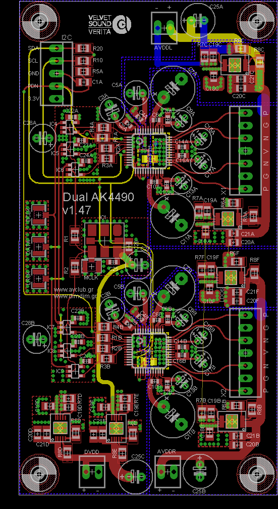
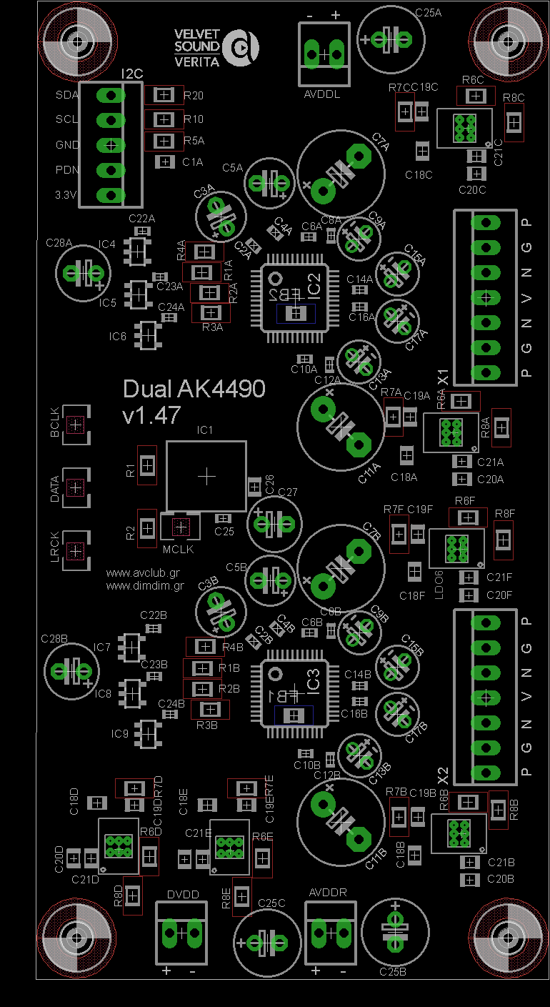
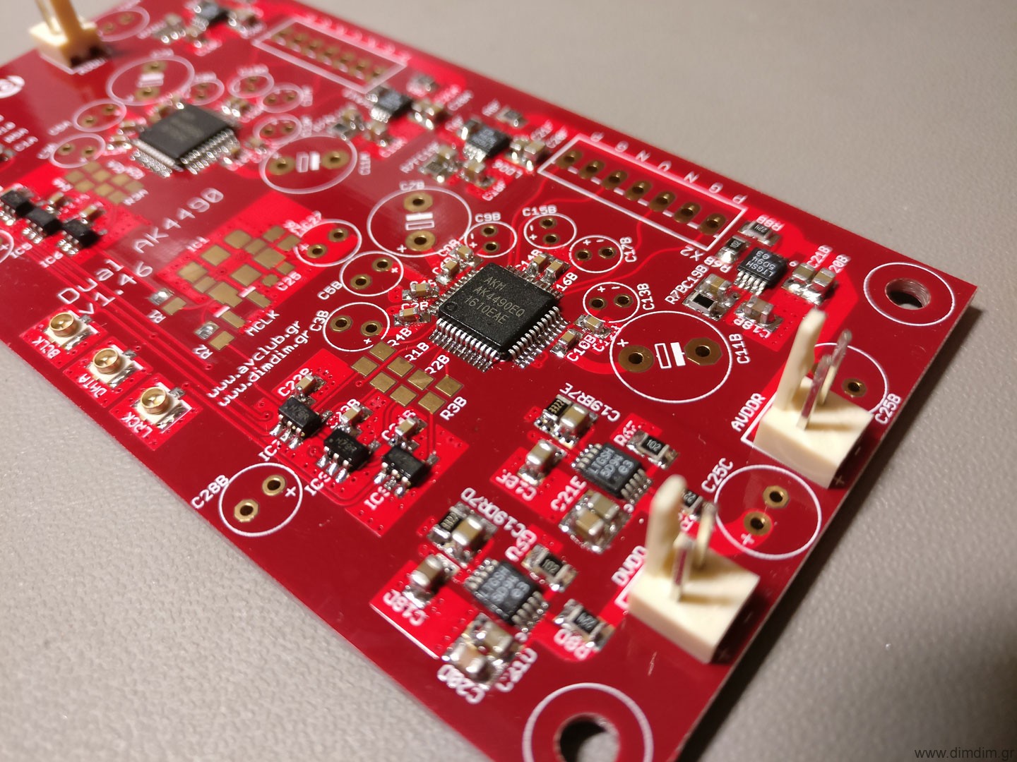
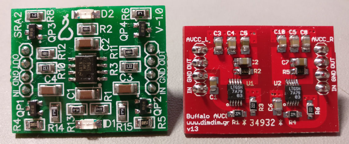
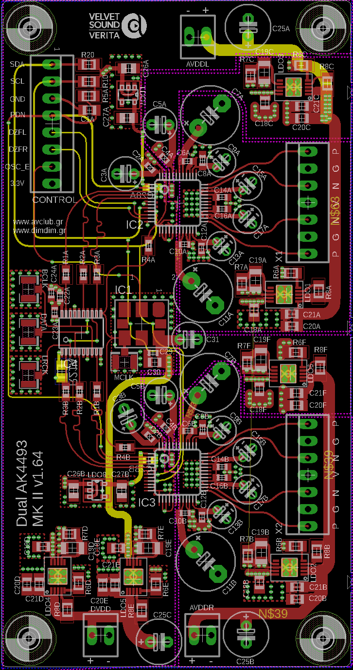
This is the 4-layer PCB:
 And this is the BoM (v1.9) in xls format:
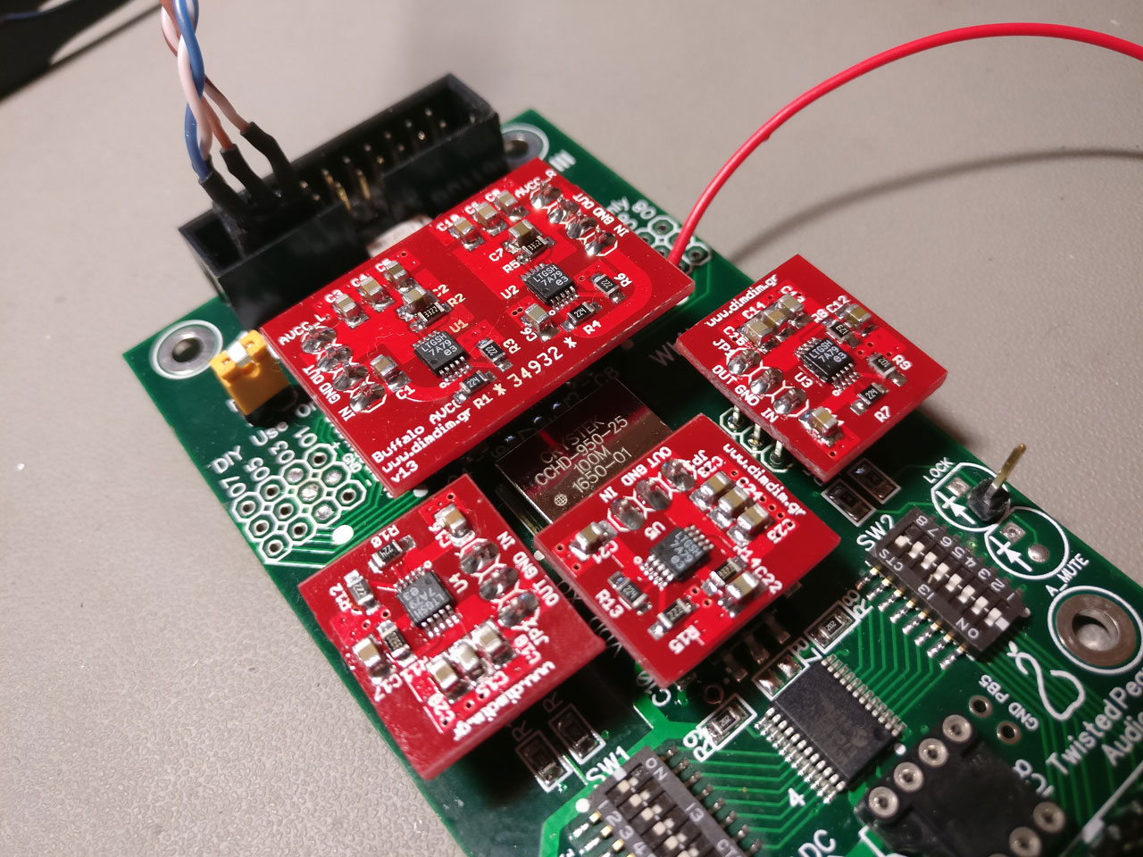
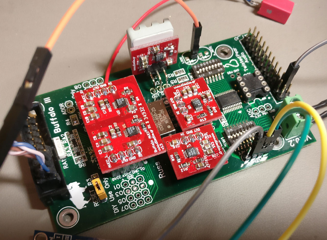
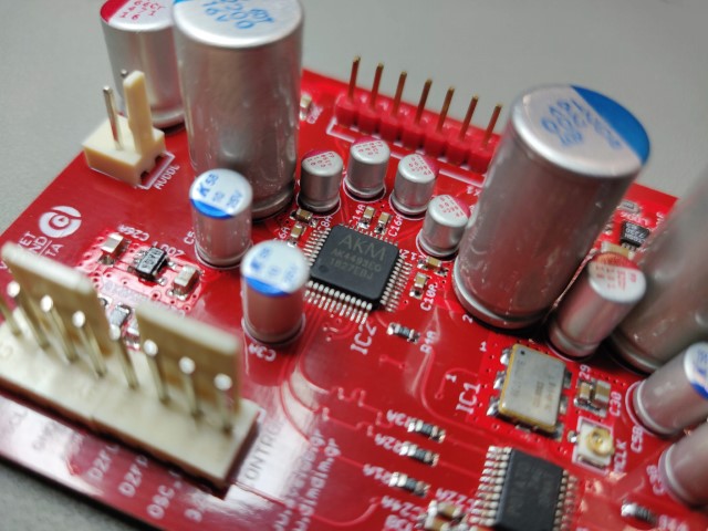
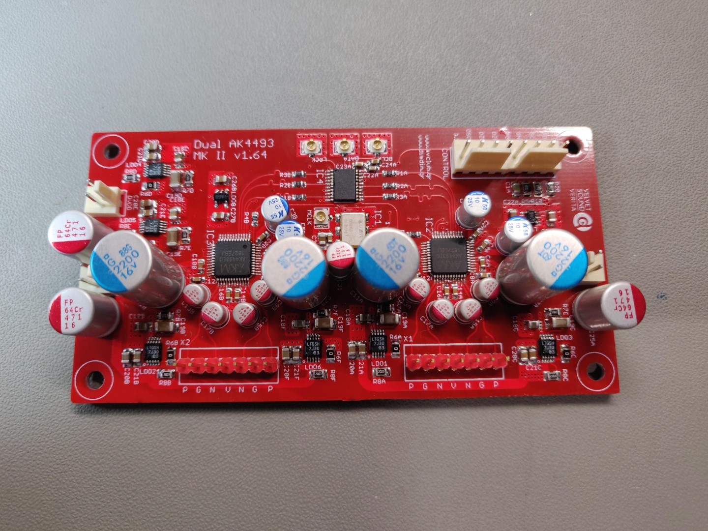
The finished board looked like this:
 The design consideration, powering scheme and clocking considerations remain the same as with the original design. There is not much sense in repeating the same text here. I will make a few notes though, based on the experience gathered from building, testing and listening to several such DACs.
- Reclocking is indeed a good idea, offering both measurable improvement in jitter as well as better sound quality.
- The pre-regulators that power this board matter. A lot. Especially the ones for AVDDL & AVDDR. We got the best (audible) results by using a couple of paralleled LT3045s.
- In a resolving system, any change in anything makes audible differences. I was particularly surprised to hear how much of a difference having correct (and uniform across my devices / stereo components) electrical phase in my power cords made.
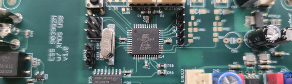
Also, having a properly designed and implemented USB to I2S receiver is very important. Early on I realized that it would be best if I designed my own XMOS-based receiver board, custom tailored to my needs. It would also include some light USB line conditioning and an AK4118-based S/PDIF receiver with 4+2 inputs. I would then standardize my DAC designs with this inputs board in mind, including properly supporting it in my Arduino code.
And so this board came to be:
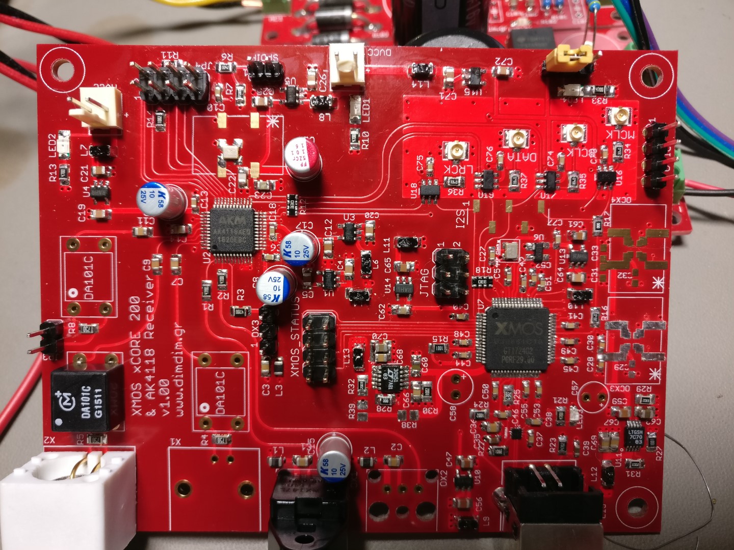 Describing in detail this board is beyond the scope of this post, but suffice it to say, building it is not for beginners. Plus you will need XMOS’ xTAG programmer to burn firmware into the XMOS chip. If anybody is feeling particularly adventurous, drop me a line and I’ll see if I have any PCBs left.
Now, regarding the Arduino code needed to control this board(s), it is not very different than that used to control the AK4490s. The main differences are:
- It has been adapted to enable the AK4493s’ PCM/DSD auto detection feature
- It has support for all of the AK4493’s digital filters
- It has support for triggering a muting relay
- It now supports the Si544 instead of the Si570
- It offers full compatibility with my XMOS / SPDIF board.
There are a number of to-do’s though, such as displaying the bit depth of the incoming PCM signal (from the USB port), plus more information on the incoming DSD stream (such as whether it is in DoP or Native format).
The hardware of the controller is the same that was used with the Dual Mono AK4490 DAC.
In this download I am including the modified versions of the libraries (as mentioned in the above linked post) as well as the necessary font files. Be sure to extract the contents of “Libraries (place in Libraries folder)” to your Arduino IDE’s “libraries” folder.
Download it here:
Regarding the output stage, it is the same design that was used for the AK4490 DAC. However its output level is slightly lower than that of the AK4490 board since the AK4493’s VREF voltage is limited to 5.25V, compared to about 7V of the AK4490. This difference in volume is easy to compensate for by changing a few resistors on the output stage.
Here is a pic of the 3 boards in action: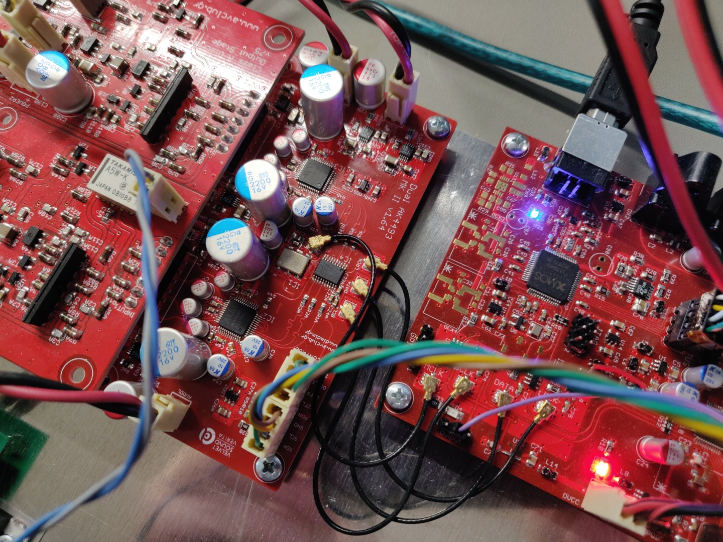 At the time of this writing there have been built 4 DACs based on this updated DAC design PCB.
If anybody is interested in building this DAC drop me a line. I have a few spare boards lying around.