The Commodore Amiga 600 was a force to be reckoned with when it was released back in 1992. It was a low-cost but very capable gaming machine. That is why it still has a loyal following.
A friend of mine belongs to the vintage gaming crowd and as such is the proud owner of an A600. Unfortunately for him, eventually his A600 gave out. After some googling he came across a number of A600 owners who have had the same problem with their units. Most of them were able to bring their machines back to life by replacing the electrolytic capacitors of the mainboard. A “re-capping kit” is relatively low-cost so my friend went ahead and ordered one. When it came he took his machine and paid me a visit.
The re-capping process ended up taking a lot longer than I had expected, but that was due to my inexperience with the specific machine. In the process I gathered a lot of information that may be of use to others, so here goes.
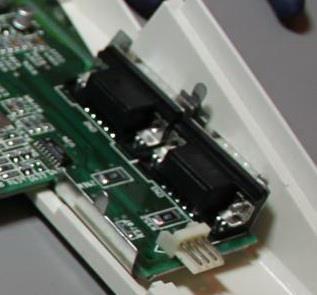
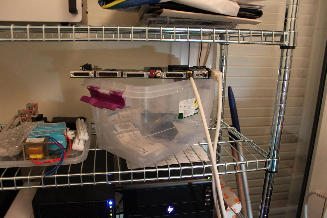
The first step is opening up the case. You do that by removing the screws on the underside of the machine and then carefully popping it open. There are a number of plastic clips on the inside of the case that need to be pried open with care. You can see a few of them in this picture (top part):
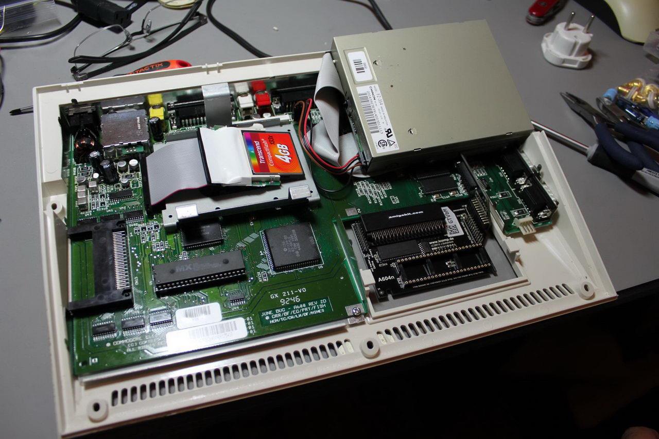
Looking at this picture you will also notice that my friend has put in a 1MB RAM upgrade as well as an HDD emulator (the 4GB flash drive).
After you have opened up the case you need to remove the mainboard. To do that you have to remove the one screw visible on the lower edge of the mainboard. After that you must lift the mainboard along with its metal shield from the right side, clearing the two ports. You will need to use a little force. Be careful – these plastics are over 20 years old and thus do break easily. When you have cleared the right side you pull the board towards the front of the case and then up so as to clear the rear connectors. Now you have removed the board from the plastic case.
Now you need to separate the mainboard from its metal shielding. To do that you take out this pesky little screw:
Then you have to unscrew the hex screws on the rear connectors. There are 8 of them in total. I haven’t taken a pic of them but they are pretty easy to spot.
Now all you have to do is bend out of the way the little pieces of metal that are situated around the shield, like this one:
Assuming all has gone well, you should have the mainboard out and be ready to start the procedure.
There is a number of caps that need to be changed. There are 4 through-hole components and a number of SMD parts.
I have circled the offending caps in this pic:
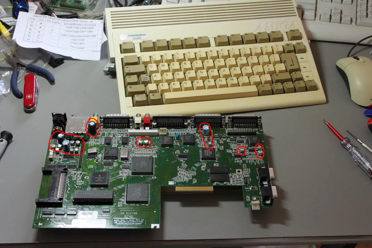
Some people choose to also change the two caps located on the back of the audio out ports. These caps are just DC blocking caps, they are not to blame for the death of the machine. Plus, they are located in a very tight spot, making replacing them too risky of a procedure.
So, first I took out the through-hole parts. That was relatively easy. Just bear in mind that you will need a relatively powerful soldering iron since the (-) sides are soldered to the ground plane which is extremely efficient at sinking heat.
Next up were the SMD parts. I had desoldered SMD caps in the past with no difficulty using a regular soldering iron but these ones proved to be particularly nasty. My first attempt ended in me pulling out one of the solder pads. I said to myself “bad luck.. whatever..” and moved on to the next cap. You guessed it – the next one also had the same luck. At that point I decided to change strategy and go with the hot air rework station. It proved to be much better at desoldering the old caps. For some reason even with the hot air I managed to pull off one SMD pad.
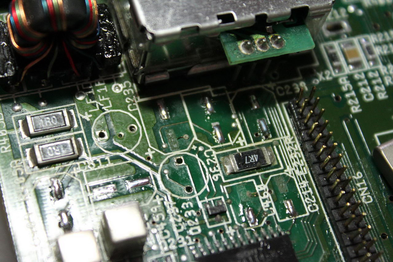
So now I had 3 caps missing pads. That is considered bad. I decided to go to the schematics and see if I could get away with not replacing the specific caps. It turns out that I was lucky. The rightmost cap (C214) is a DC blocking cap that sends the summed L+R audio to the RF encoder IC. Since my friend does not (and will never) use the RF modulator, it was OK to not care about this cap.
I was not so lucky with the next one, C460. This cap is used to bypass the U12 IC, which I’m afraid is actually necessary for proper operation of the board. So I had to get creative. The missing pad corresponds to the GND connection, so I thought I would just solder some wire from the bottom of the cap to a nearby GND point. It turned to be much easier than that. I scraped the green lacquer from the remaining trace and managed to solder the capacitor to that by turning it a bit. In other words, I got lucky.
With the third cap (C235) I did what I did with the second one – scraping off the lacquer and soldering at a small angle. After I had done the procedure I remembered to look at the schematic to see what it was for – it turned out that I could have gotten away with not installing it since it was also a DC blocking capacitor, this time from the encoder IC to the RF modulator module. Oh, well..
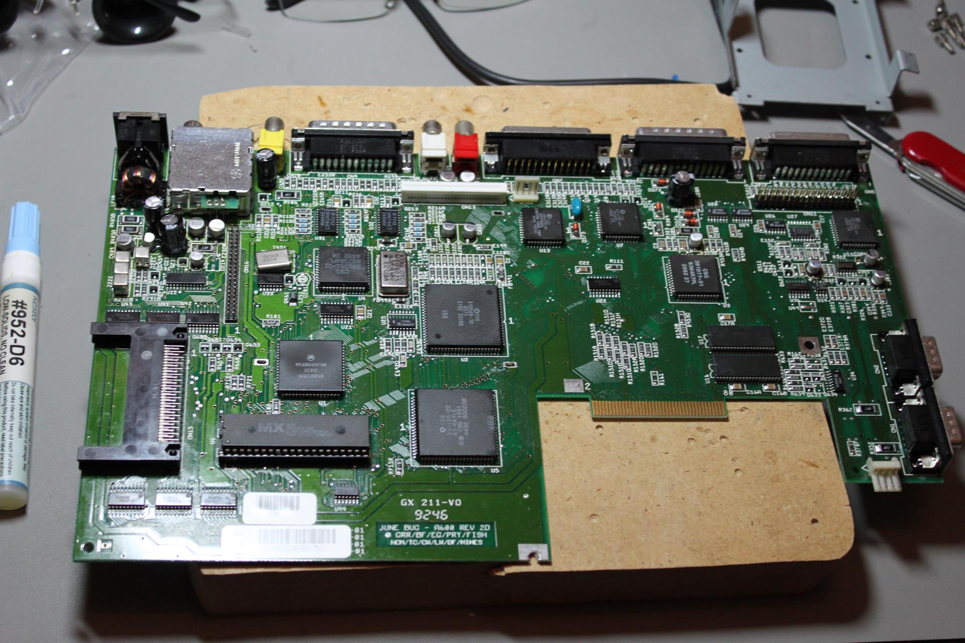
When I was done the board looked like this:
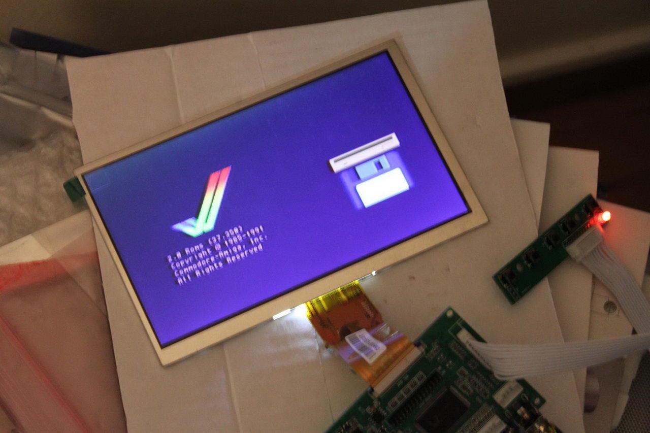
This was the moment of truth. We hooked up the board to its power supply and my (very bare) test display.
We plugged in the power and voila! The Amiga 600 lives! 🙂
We then proceeded to put the machine back together and do another test, this time with the HDD installed. As was expected, everything was working just fine:
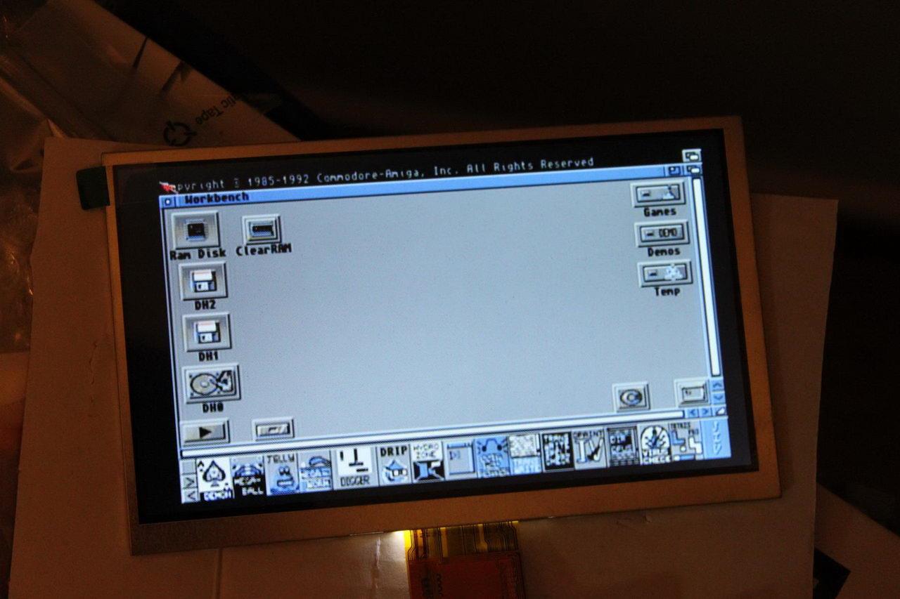
So, there you have it. An (almost) fully re-capped Amiga 600. My friend is in for some serious gaming. 🙂