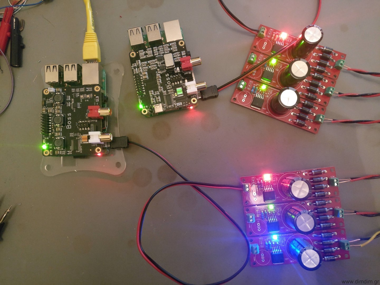
For the better part of a year I’ve been busy developing what one would call a “respectable” DAC from scratch. It has been a team effort, with different people becoming more involved with specific aspects of the project, but pretty much everyone involved ended up learning a lot about DACs. Right now, the project is for the most part finished, in that it is fully functional with a USB input and a pair of single ended outputs (or balanced, if you use a passive transformer-based stage). It is controlled by an Arduino-compatible micro-controller, running my aKduino v2 code (more on that in a future post).
I will do a series of posts detailing the design and build process, with each post covering a specific PCB. When the series is complete, the contents of all of the posts will be concatenated into a project page.
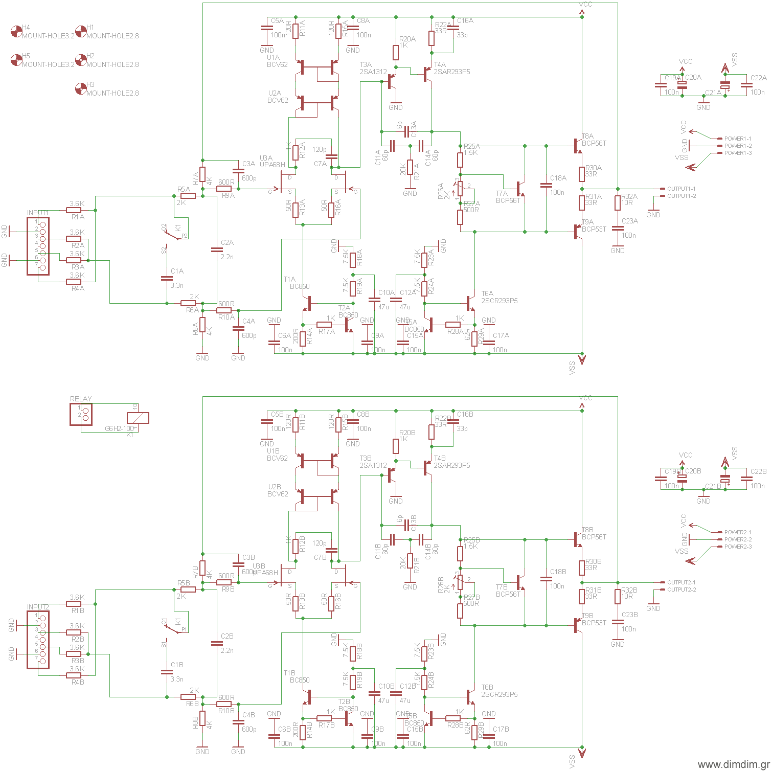
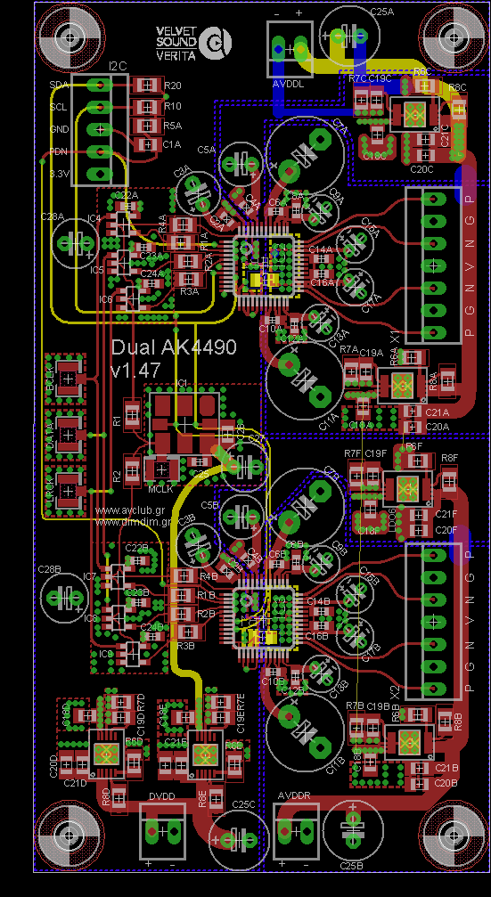
So, without further ado, this is the schematic of the main DAC board:
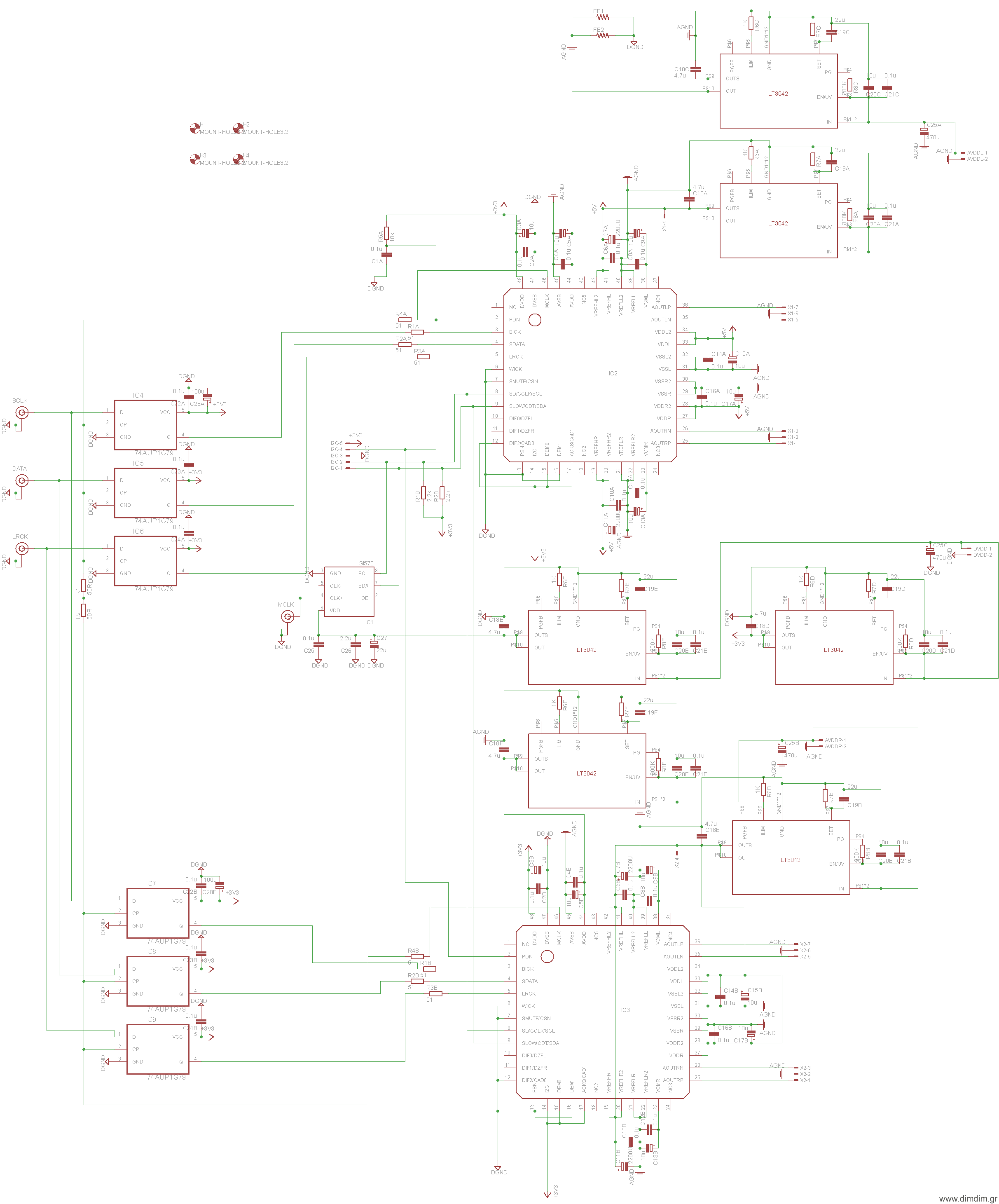 (Right click, Save Image As.. to download it in full resolution)
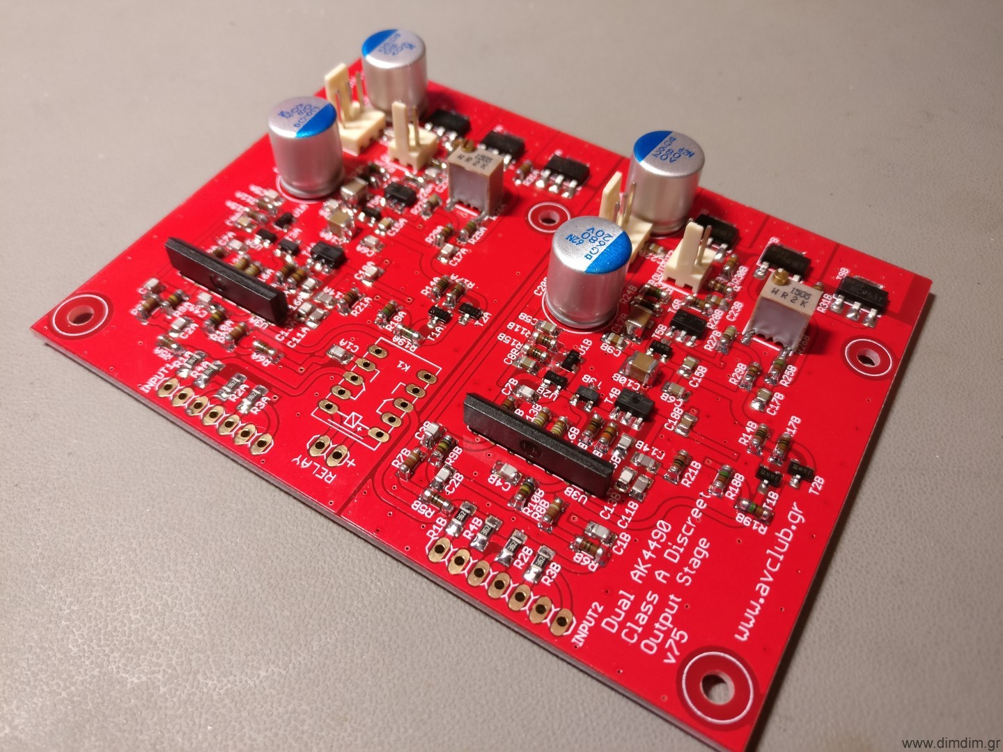
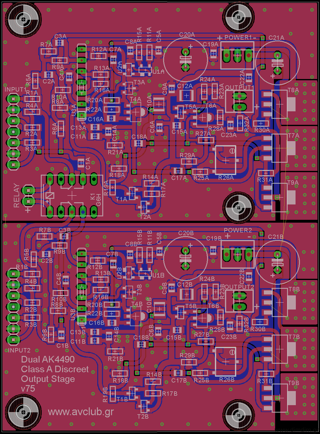
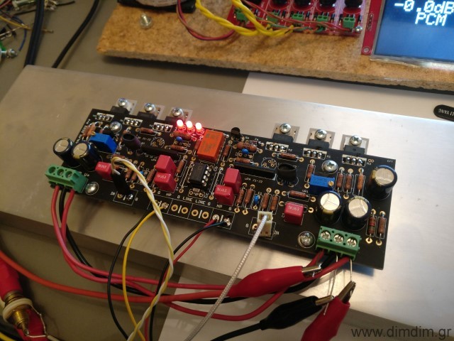
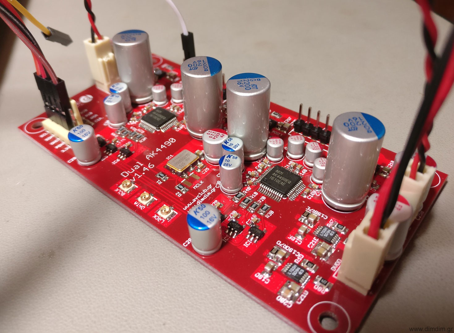
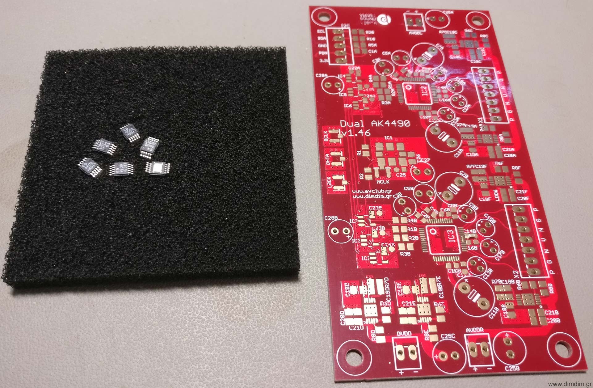
This is the 4-layer PCB:
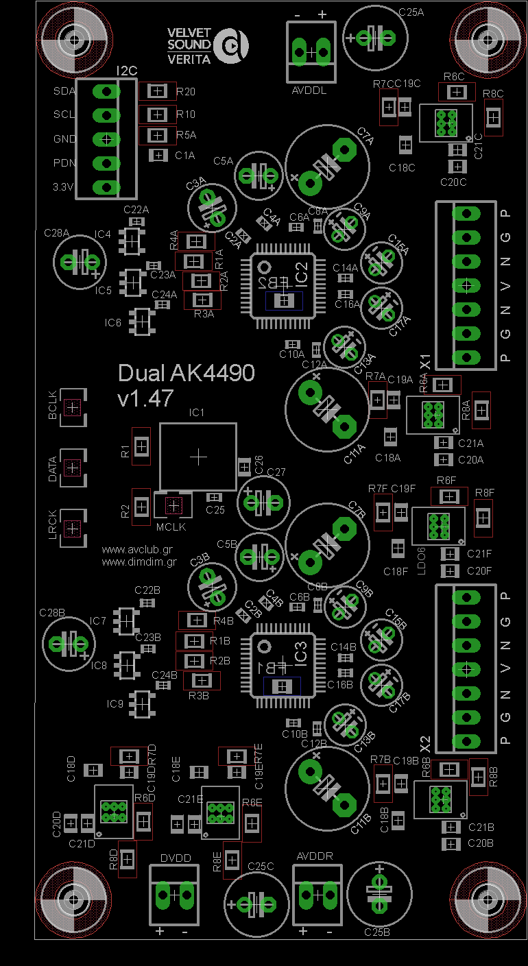
This is the parts placement diagram:
And this is the BoM (v1.9) in xls format:
Dual AK4490 DAC (main board BoM) (19359 downloads )
Design considerations
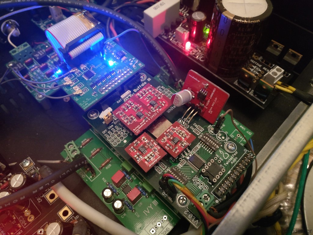
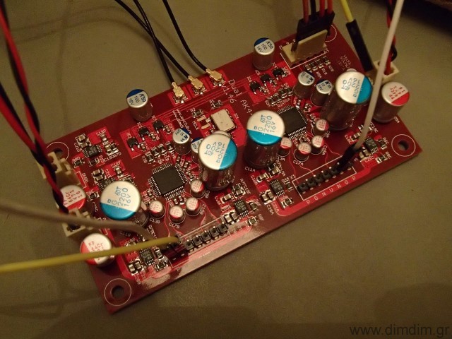
The design goal was to do a dual mono design so as to maximize SNR and channel separation. A 4-layer PCB design was chosen so as to have a very solid, low impedance ground plane as well as proper power and signal planes. The I2S, audio signals and power after the local LDO regulators are routed on the top layer, the 2 middle layers are ground and power planes, and the bottom layer serves to route I2C signals and some power lines.
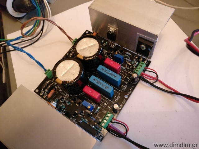
Power
All of the local power supplies are implemented using the currently top-of-the-line LT3042 LDOs. The VDDL & VDDR (analog power supplies) are set to 7.2V so as to maximize SNR and dynamic range. There is provision for providing separate pre-reg power supplies for the L and R channels (headers AVDDL and AVDDR) but I don’t consider that to be critical to SQ since there are local LDOs and the power draw is very very small. In my implementation I’m using a common pre-reg for both the AVDDL & AVDDR. The AVDDs and DVDDs are also supplied by LT3042 LDOs set to output 3.3V. The Si570 has its own dedicated 3.3V supply implemented with an LT3042 and features extra filtering.
Overall, the power requirements of the board are:
1) AVDDL: 8-10V DC at 40mA max
2) AVDDR: 8-10V DC at 40mA max
3) DVDD: 4-6V DC at 200mA max
Clocking & input signals
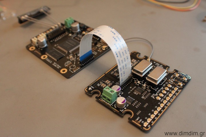
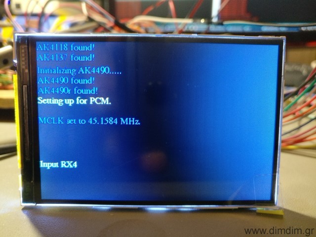
It was decided that the MCLK would be provided by a programmable low jitter oscillator, namely the Si570. This way we could select different MCLK frequencies at will, supporting different sampling rate families and different USB to I2S boards.
Speaking of USB to I2S boards, the DAC board has a very specific requirement: The USB board must be able to receive MCLK externally. In other words, the DAC board and USB board must be clocked from the same oscillator. This is due to the AK4490’s design. Unlike the ESS designs which by default run asynchronously, it needs to be on the same clock domain as its I2S sources.
So, the DAC board needs to output MCLK back to the USB board. There exist a number of USB boards that support that. The most popular ones are the Amanero Combo384 and JLsounds’ I2SoverUSB.
Since I had decided to do reclocking using flip-flops as close to the AK4490s as possible, and the flip-flops are clocked by the MCLK, its frequency needs to be sufficiently high in order to reclock signals corresponding to high sample rates. This translates to 49.152 MHz for sampling rates of 384KHz. If you’re content with going only up to 192KHz, you can use a MCLK of “just” 24.576 MHz. Of course you will also need the corresponding MCLKs of 45.1584 and 22.5792 MHz for the 44.1K families of SRs.
If you decide that you don’t want to do reclocking on the DAC board, you can just not solder on the flip-flops and just connect the proper pads together with some wire so as to bypass them. That way you can run with 22.5792 & 24.576 MHz clocks with SRs up to 384KHz (and probably beyond..).
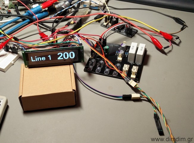
If you decide that you would also prefer to not use the Si570 and just clock the DAC board directly from your USB to I2S board (or other suitable I2S source) you can also do that. You just don’t solder-on the Si570 and make a couple of changes to the Arduino code (to be implemented..).
But I urge you to try the Si570 & reclocking way first..
Construction hints
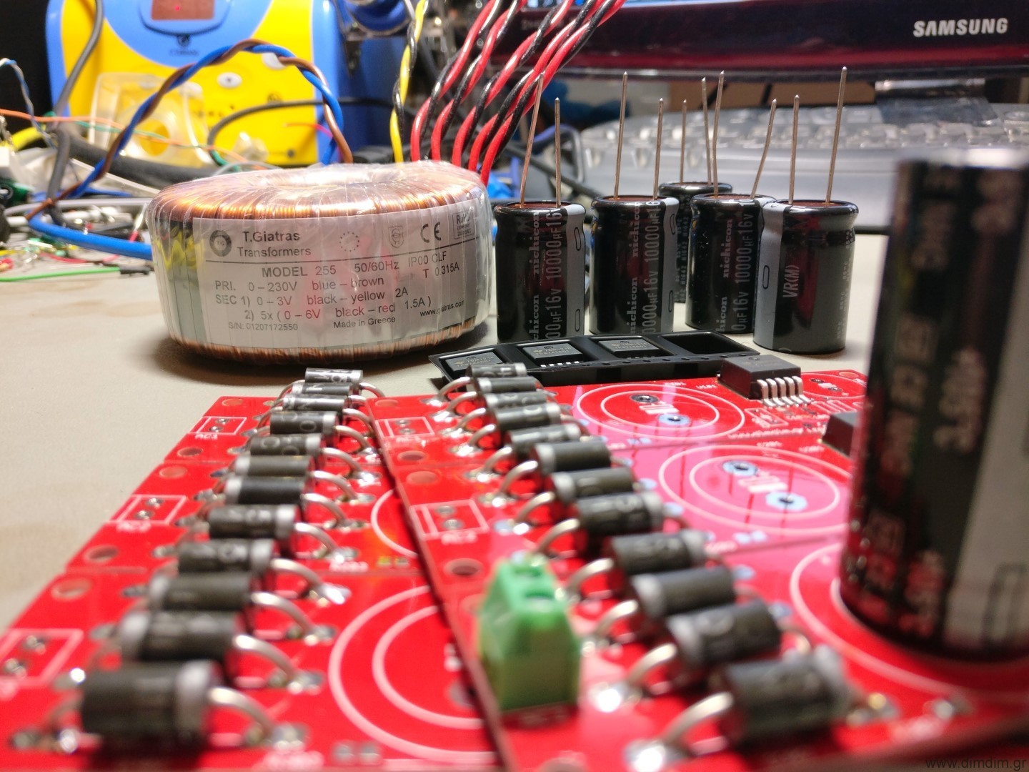
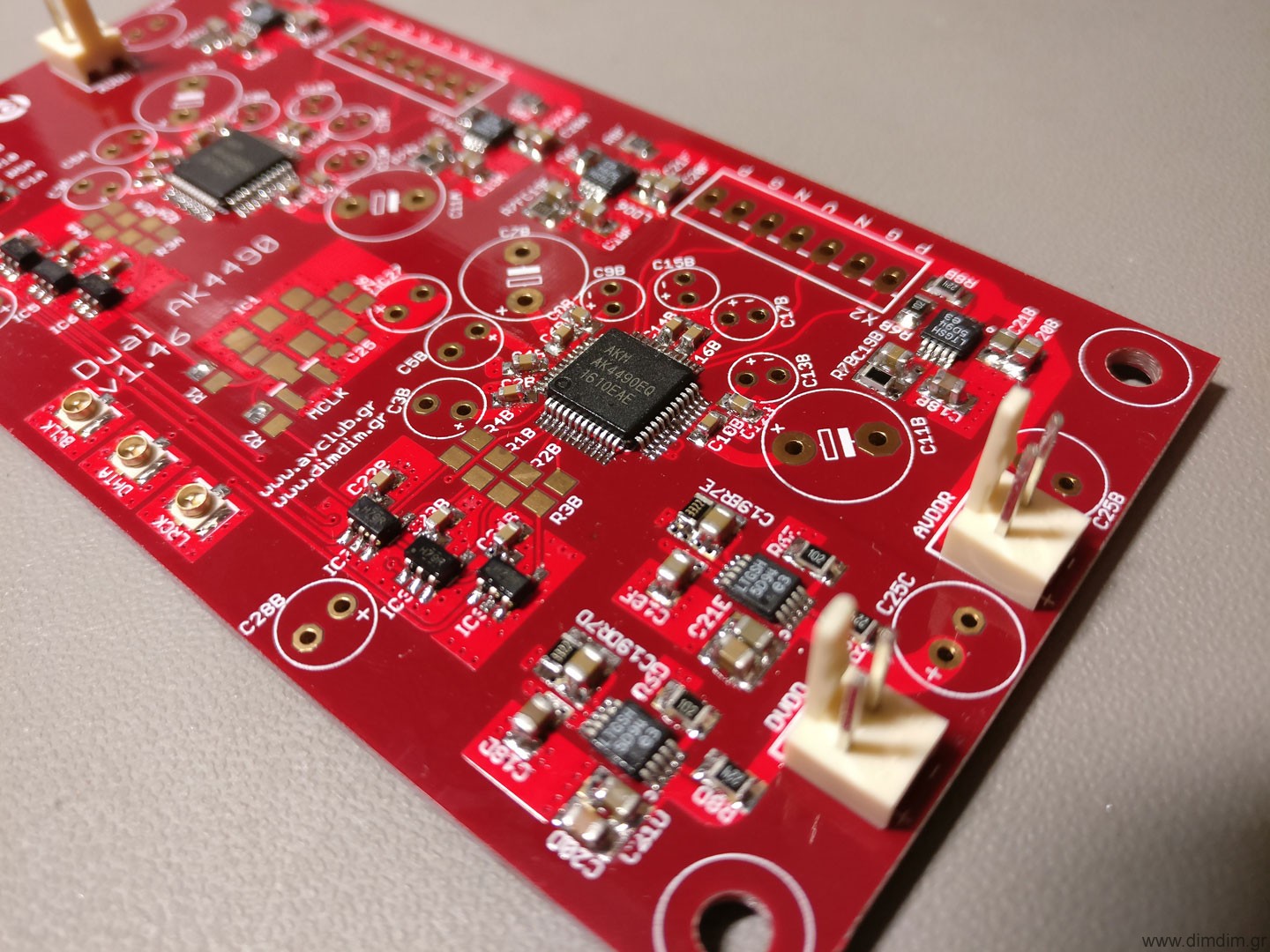
Start by first soldering on the power supply components (LDOs, resistors, caps, etc.) and testing that everything works the way that it should.
The LT3042s are pretty tiny and its easy to make a mistake while soldering them. I’ve found that the easiest method is by using a hot air rework station. First I use a regular soldering iron to tin the thermal pad and the pads with a small amount of solder. Then I apply a good amount of high quality solder paste, put the LDO on top of the pads and heat the area of the board until the solder melts. I set my hot air station to a relatively low temp of ~280 degrees C and the process takes less than a minute (per LDO). But you could also solder them with a soldering iron. To solder the heatpad, warm up the pad from the underside of the board and add solder.
After the power section, you should solder on the AK4490s and other low profile components. I do that with a low power (18W) soldering iron with a fine tip.
Next up is the Si570 programmable oscillator. I start by putting a little solder on one of the pads:
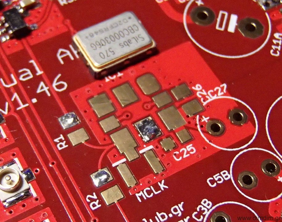
Then I add soldering paste and I place the Si570 on top of the pads. I use the fine tipped soldering iron to melt the solder on the tinned pad, effectively soldering the Si570 on the board. I then proceed to solder the rest of the pads by applying heat with the soldering iron to the side of the pads of the Si570 and adding solder.
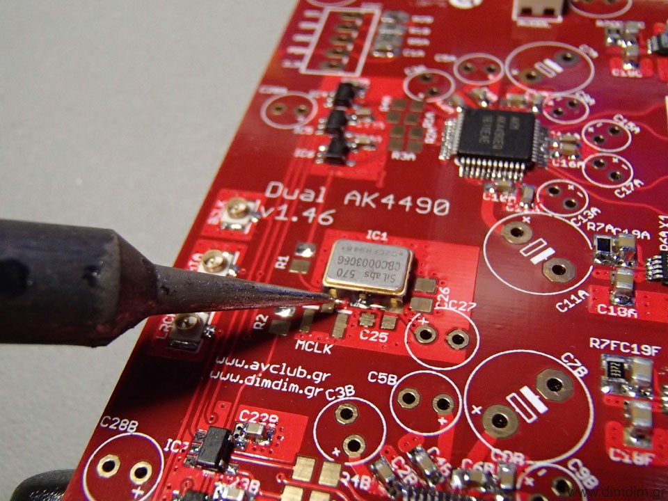
You should finish up by soldering the electrolytic capacitors and other higher profile parts.
Beware that the spacing around the electrolytics is very tight. You should take that into account when selecting parts. The parts in the BoM are sure to fit in the available space.
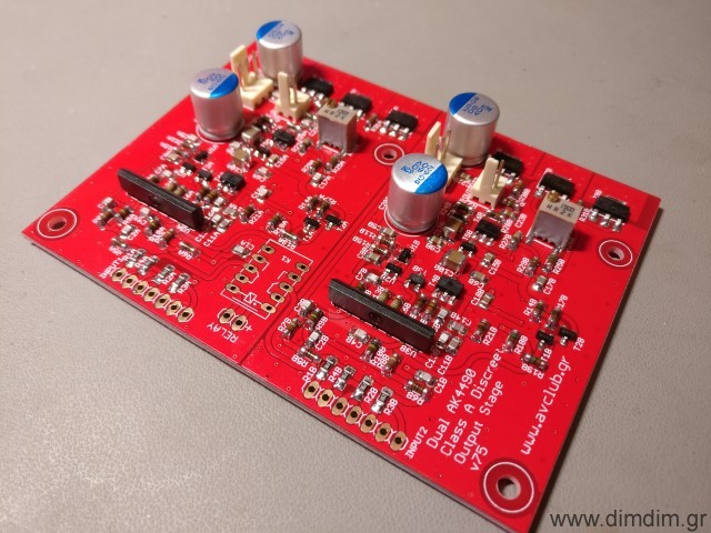
That’s it for Part 1. Stay tuned for Part 2: The Controller.